Shallow trench isolation structure and manufacturing method thereof

A technology of isolation structure and manufacturing method, which is applied in semiconductor/solid-state device manufacturing, electrical components, circuits, etc., can solve the problems of shortening the moving path, reducing isolation performance, and damaging the isolation performance of semiconductor devices, so as to achieve the effect of ensuring isolation

Active Publication Date: 2015-09-09
SEMICON MFG INT (SHANGHAI) CORP
View PDF3 Cites 0 Cited by
  • Summary
  • Abstract
  • Description
  • Claims
  • Application Information

AI Technical Summary

Problems solved by technology

When the edge of the photoresist layer 104 is shifted to one side of the P-type well region 102B, the N-type well region 102A formed by the ion implantation process using the photoresist layer 104 as a mask will move toward the side of the P-type well region 102B. One side is shifted, and even the N-type well region 102A crosses the shallow trench isolation structure 101, which will cause the movement path N-N of electrons between the N-type well region 102A and the drain / source electrode 103B of the MOSFET transistor to be shortened, resulting in isolation performance Reduce and impair the isolation performance of semiconductor devices
By the same token, when the edge of the photoresist layer (not shown) forming the P-type well region 102B is shifted to one side of the N-type well region 102A, holes will be generated in the P-type well region 102B and the source of the MOSFET transistor. / drain 103A travel path is shortened, while degrading the isolation performance

Method used


Image

  • Shallow trench isolation structure and manufacturing method thereof
  • Shallow trench isolation structure and manufacturing method thereof
  • Shallow trench isolation structure and manufacturing method thereof

Examples


Embodiment Construction

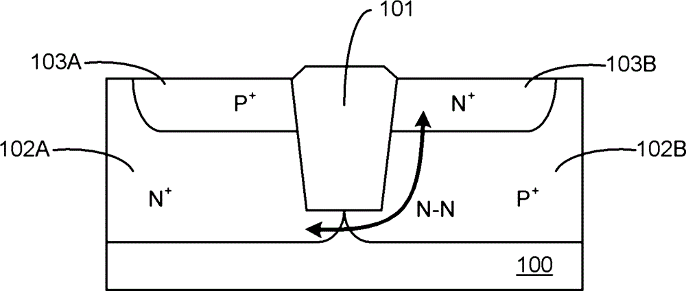
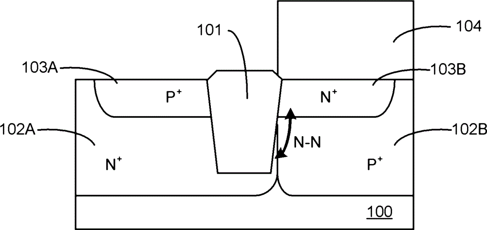
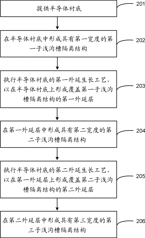
[0023] Next, the present invention will be described more fully with reference to the accompanying drawings, in which embodiments of the invention are shown. However, this invention may be embodied in different forms and should not be construed as limited to the embodiments set forth herein. Rather, these embodiments are provided so that this disclosure will be thorough and complete, and will fully convey the scope of the invention to those skilled in the art. In the drawings, the size and relative sizes of layers and regions may be exaggerated for clarity. Like reference numerals refer to like elements throughout.

[0024] It will be understood that when an element or layer is referred to as being "on," "adjacent," "connected to" or "coupled to" another element or layer, it can be directly on the other element or layer. A layer may be on, adjacent to, connected to, or coupled to other elements or layers, or intervening elements or layers may be present. In contrast, when a...


PUM


Abstract

The invention provides a shallow groove isolation structure and a manufacturing method thereof. The manufacturing method comprises the steps as follows; providing a semiconductor substrate; forming a first sub shallow groove isolation structure with a first width in the semiconductor substrate; forming a first epitaxial layer for covering the first sub shallow groove isolation structure on the semiconductor substrate; forming a second sub shallow groove isolation structure with a second width in the first epitaxial layer, wherein the second sub shallow groove isolation structure is located above the first sub shallow groove isolation structure, and the second width is larger than the first width; forming a second epitaxial layer for covering the second sub shallow groove isolation structure on the first epitaxial layer; and forming a third sub shallow groove isolation structure with a third width in the second epitaxial layer, wherein the third sub shallow groove isolation structure is located above the second sub shallow groove isolation structure, and the third width is smaller than the second width. The shallow groove isolation structure is cross-shaped, so that a movement path, between a trap region and a source / drain electrode of a transistor on the opposite side of the trap region, of a carrier is guaranteed so as to guarantee the isolation.

Description

technical field [0001] The invention relates to the technical field of semiconductor manufacturing, in particular to a shallow trench isolation structure and a manufacturing method thereof. Background technique [0002] Shallow trench isolation (STI) technology is currently the main method used for device isolation in the manufacture of large-scale integrated circuits. As semiconductor technology enters the deep submicron era, devices below 0.13 microns, such as MOSFET (Metal Oxide Semiconductor Transistor) devices, use shallow trench isolation structures between the body region and the drift region. [0003] Figure 1A It is a cross-sectional view of a MOSFET device formed with a shallow trench isolation structure in the prior art. Such as Figure 1A As shown, a shallow trench isolation structure 101 is formed in the semiconductor substrate 100 , and an N-type well region 102A and a P-type well region 102B are respectively formed on both sides of the shallow trench isolati...

Claims


Application Information

Patent Timeline
Patent Type & Authority Patents(China)
IPC IPC(8): H01L21/762
Inventor 刘金华
Owner SEMICON MFG INT (SHANGHAI) CORP
Why Eureka
Try Eureka