Array substrate, repair method for broken lines of array substrate and display device

一种阵列基板、栅线的技术,应用在阵列基板,断线修复方法及显示装置领域,能够解决条数限制、影响液晶显示产品良率、断线修复线数量有限等问题,达到提高产品良率的效果

Active Publication Date: 2013-09-04
BOE TECH GRP CO LTD +1
View PDF6 Cites 34 Cited by
  • Summary
  • Abstract
  • Description
  • Claims
  • Application Information

AI Technical Summary

Problems solved by technology

However, if this method is used to repair the array substrate, due to the limited number of disconnected repair lines 9, there is a limit to the number of data lines to be repaired, and generally two disconnected data lines can be repaired at most.
Moreover, there is no mature method for repairing broken wires of grid lines at present.
If the disconnection of the array substrate cannot be effectively repaired, it will affect the yield of liquid crystal display products

Method used


Image

  • Array substrate, repair method for broken lines of array substrate and display device
  • Array substrate, repair method for broken lines of array substrate and display device
  • Array substrate, repair method for broken lines of array substrate and display device

Examples


Embodiment Construction

[0038] The specific embodiments of the present invention will be described in detail below in conjunction with the drawings.

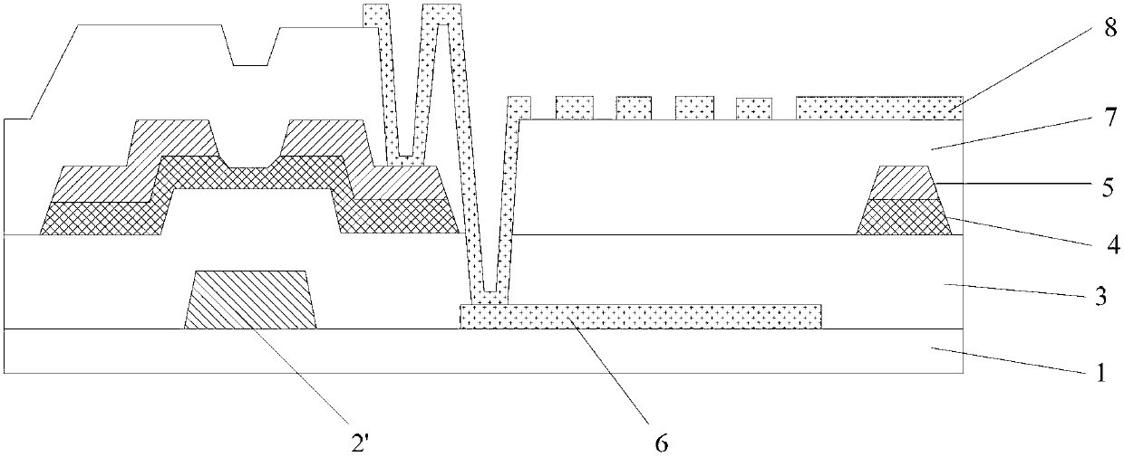
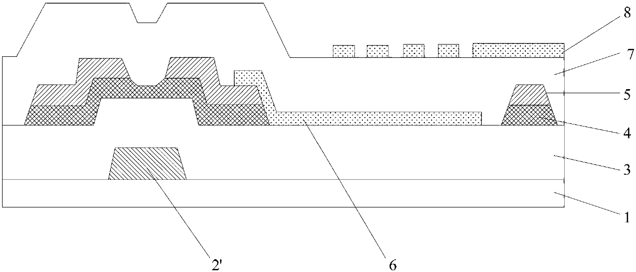
[0039] This embodiment provides an array substrate, such as HADS type or ADS type liquid crystal array substrate, such as figure 1 , Figure 4 with Figure 5 As shown, it includes a common electrode 8, a pixel electrode 6, a gate line 2 and a data line 5. The gate line 2 and the data line 5 are both covered with a common electrode 8, and the gate line 2 and the data line 5 are arranged to form multiple Pixel regions arranged in a matrix, the common electrode 8 is provided with a pattern of a plurality of strip-shaped hole structures 8a above each pixel region, the gate line 2, the data line 5 and the common electrode 8 are made in different The layers are partially overlapped with each other, and the common electrode 8 is provided with a pattern of the first hole structure 12 at the corresponding position where the gate line 2 and the data line 5 intersect...


PUM


Abstract

The invention relates to liquid crystal display devices, in particular to an array substrate, a repair method for broken lines of the array substrate and a display device. The array substrate comprises a common electrode, pixel electrodes, thin film transistors, grid lines and data lines, wherein the grid lines and the data lines are arranged in a crossed mode to form a plurality of pixel areas which are arranged in a matrix mode, a plurality of patterns which are of a strip-shaped and hole-shaped structure are respectively arranged the common electrode above each pixel area, the grid lines, the data lines and the common electrode are manufactured on different layers and mutually overlap with one another in a partial mode, and a pattern which is of a first hole-shaped structure is arranged at the position, corresponding to the crossed position of each grid line and each date line, of the common electrode. Due to the design of the patterns of a common electrode layer, the broken lines of the data lines and the grid lines on the array substrate can be conveniently and rapidly repaired, limitation of the number of the broken lines is overcome by repair of the broken lines of the data lines, and product yield of the array substrate is effectively improved.

Description

Technical field [0001] The present invention relates to a liquid crystal display device, and in particular to an array substrate, a method for repairing broken wires of the array substrate, and a display device. Background technique [0002] In the manufacturing process of liquid crystal display panels, repairing broken wires is an important means to improve yield. In the prior art, a structure of laying data repair lines around the liquid crystal display panel is generally adopted to facilitate repair of broken grid lines. [0003] ADS-type liquid crystal panel (Advanced-Super Dimensional Switching; Advanced Super Dimensional Switching Technology) forms a multi-dimensional electric field through the parallel electric field generated by the edge of the pixel electrode or the common electrode in the same plane and the longitudinal electric field generated between the pixel electrode and the common electrode. All the aligned liquid crystal molecules between the pixel electrode or th...

Claims


Application Information

Patent Timeline
Patent Type & Authority Applications(China)
IPC IPC(8): G02F1/1362G02F1/13
CPCG02F1/134363G02F1/136259G02F2201/121H01L27/124G02F1/136263G02F1/134318G02F1/1309G02F1/134309G02F1/136286G02F1/1368H01L27/1259
Inventor 吴松包杰琼
Owner BOE TECH GRP CO LTD
Why Eureka
Try Eureka