Supercharge Your Innovation With Domain-Expert AI Agents!

Liquid crystal display device, manufacturing method thereof, and electronic device

A technology of liquid crystal display device and liquid crystal layer, which is applied in the directions of optics, instruments, optical components, etc., can solve problems such as reducing brightness drop, and achieve the effect of reducing loss.

Active Publication Date: 2018-04-03
JAPAN DISPLAY INC
View PDF2 Cites 0 Cited by
  • Summary
  • Abstract
  • Description
  • Claims
  • Application Information

AI Technical Summary

Problems solved by technology

Such an LCD panel would reduce brightness drop for viewers wearing polarized sunglasses without providing a phase difference plate

Method used


Image

  • Liquid crystal display device, manufacturing method thereof, and electronic device
  • Liquid crystal display device, manufacturing method thereof, and electronic device
  • Liquid crystal display device, manufacturing method thereof, and electronic device

Examples


no. 1 example

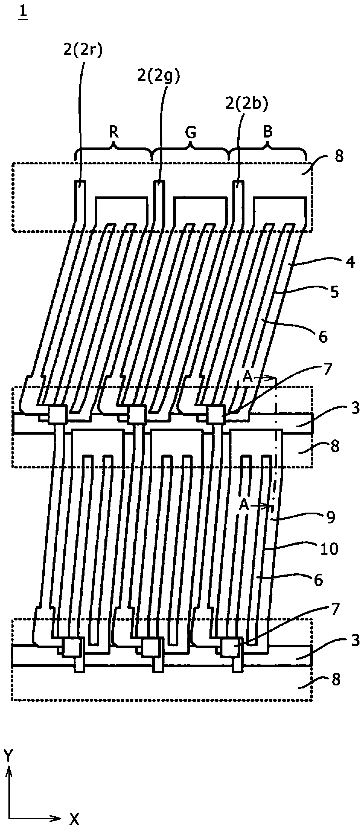
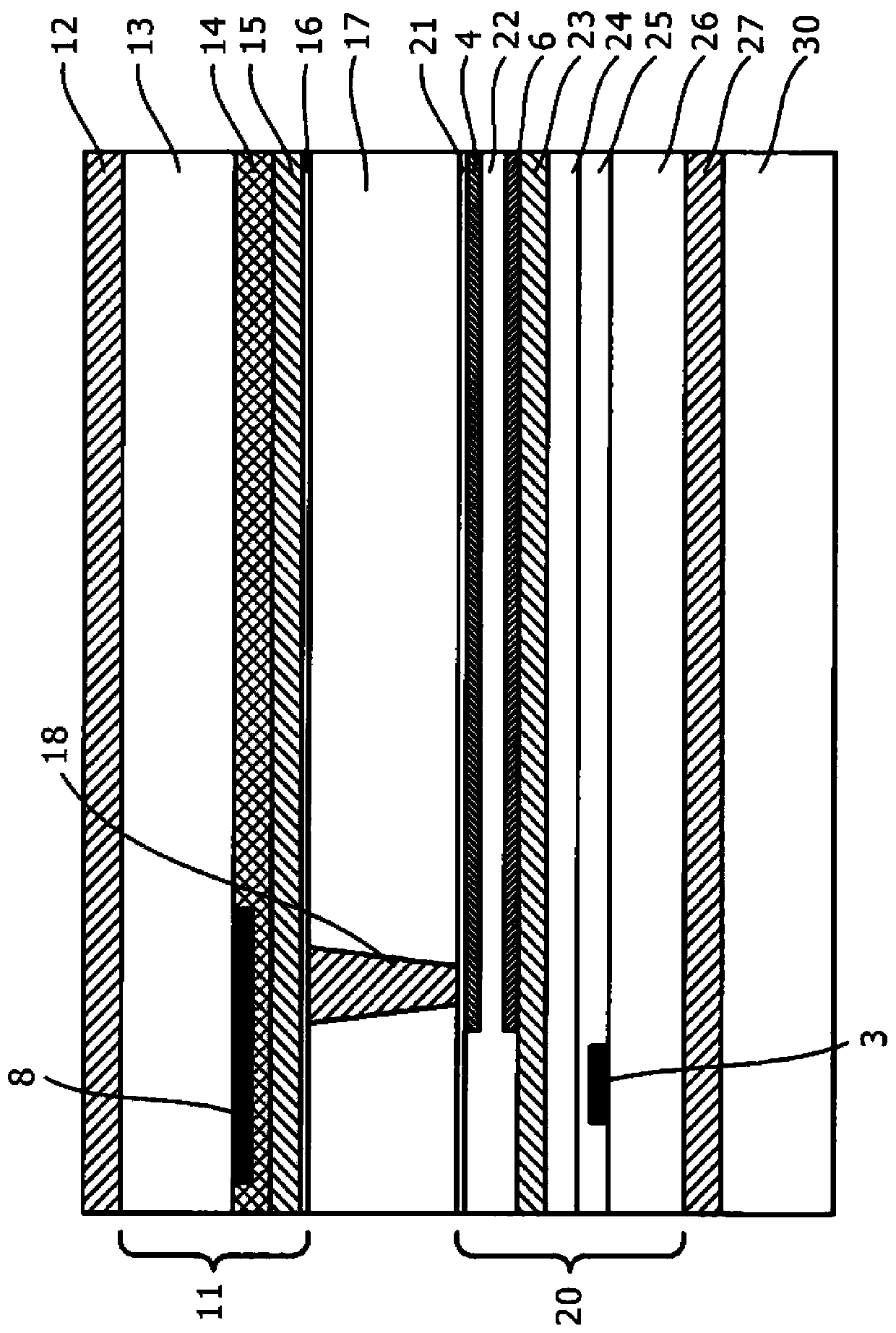
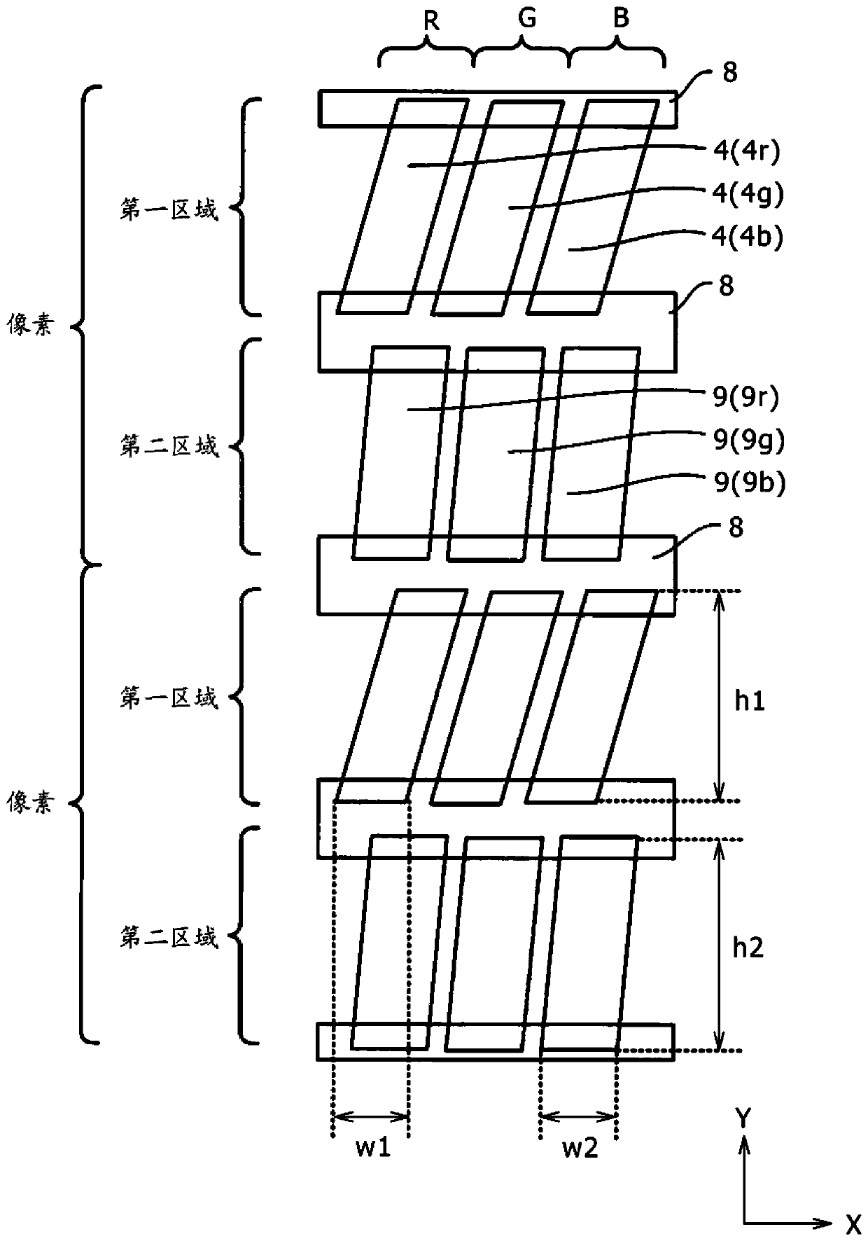
[0028] First, refer to Figures 1 to 3 A liquid crystal display panel according to a first embodiment is described. figure 1 is a schematic diagram showing a front view of a pixel of the liquid crystal display panel according to the first embodiment. figure 2 is along figure 1 A cross-sectional view taken along line A-A in . image 3 is a schematic diagram showing an alternate structure of regions constituting sub-pixels of the liquid crystal display panel according to the first embodiment.

[0029] The liquid crystal display panel (liquid crystal display device) 1 is a liquid crystal display panel of a horizontal electric field, and more specifically, a liquid crystal display panel of an FFS type. The liquid crystal display panel 1 includes a color filter substrate 11 and an array substrate 20 as a pair of substrates disposed opposite to each other. Each of the color filter substrate 11 and the array substrate 20 is made of a transparent member such as glass or plastic a...

no. 2 example

[0086] Figure 9 is an appearance perspective view showing an example of a television set according to the second embodiment. The television set 100 has, for example, a video display screen part 102 comprising a front panel 103 and a filter glass 101 . The video display screen section 102 includes the liquid crystal display panel 1 according to the first embodiment.

no. 3 example

[0088] Figure 10A and 10B is an appearance perspective view showing an example of a digital camera according to the third embodiment. Figure 10A is a three-dimensional view of the appearance viewed from the front side of the digital camera, while Figure 10B It is a perspective view of the external appearance seen from the rear side. The digital camera 110 has, for example, a flash section 112 , a display section 113 , a menu switch 114 , and a shutter button 111 . The display section 113 includes the liquid crystal display panel 1 according to the first embodiment.


PUM


Abstract

Provided are a liquid crystal display device, a manufacturing method thereof, and an electronic device. The liquid crystal display device includes: a plurality of scanning lines and a plurality of signal lines disposed on one of paired substrates disposed to face each other with a liquid crystal layer interposed therebetween, the plurality of scanning lines and the plurality of signal lines The lines extend in different directions; and the alignment film, the pixel electrode, the insulating layer and the common electrode are sequentially arranged from one side of the liquid crystal layer, and the alignment film is rubbed in a rubbing direction which has a given direction relative to the direction in which the pixels are arranged. fixed inclination. The pixel electrode is separated by a scan line and a signal line, and has a sub-pixel composed of a first area and a second area. The first region has a plurality of slit-shaped openings having a given inclination in the first direction with respect to the rubbing direction. The second region has a plurality of slit-shaped openings having a given inclination in the second direction with respect to the rubbing direction.

Description

technical field [0001] The present technology relates to a liquid crystal display device, a method of manufacturing the liquid crystal display device, and electronic equipment including the liquid crystal display device. Background technique [0002] An FFS (Fringe Field Switching) type LCD (Liquid Crystal Display) panel is known as an LCD panel of a horizontal electric field. LCD panels of the FFS type have been applied to portable electronic devices such as mobile phones, and such electronic devices are widely used. Portable electronic devices are often used outdoors, and the user of the device may have the opportunity to view the display screen of the portable electronic device through polarized sunglasses. At this time, if the FFS type LCD panel has linear polarization characteristics, and if the transmission axis of polarized sunglasses forms an angle of 0 degrees and 180 degrees or an angle of 90 degrees and 270 degrees with the transmission axis of the FFS type LCD p...

Claims


Application Information

Patent Timeline
Patent Type & Authority Patents(China)
IPC IPC(8): G02F1/1337G02F1/1343G02F1/1333G02F1/1362G02C7/10
CPCG02F1/133707G02F1/134363G02F2201/52G02F1/133784G02F1/1343G02F1/1337G02F1/134372G02F1/136286
Inventor 伊藤大亮大森英幸
Owner JAPAN DISPLAY INC
Features
  • R&D
  • Intellectual Property
  • Life Sciences
  • Materials
  • Tech Scout
  • Unparalleled Data Quality
  • Higher Quality Content
  • 60% Fewer Hallucinations
Learn More