Light emitting diode pixel unit circuit and display panel

A technology of light-emitting diodes and pixel units, applied in static indicators, electrical digital data processing, instruments, etc., can solve the problem of uneven brightness of display panels and achieve the effect of improving uniformity

Active Publication Date: 2013-09-18
BOE TECH GRP CO LTD +1
View PDF6 Cites 16 Cited by
  • Summary
  • Abstract
  • Description
  • Claims
  • Application Information

AI Technical Summary

Problems solved by technology

[0006] An embodiment of the present invention provides a light-emitting diode pixel unit circuit and a display panel to s

Method used


Image

  • Light emitting diode pixel unit circuit and display panel
  • Light emitting diode pixel unit circuit and display panel
  • Light emitting diode pixel unit circuit and display panel

Examples


Example Embodiment

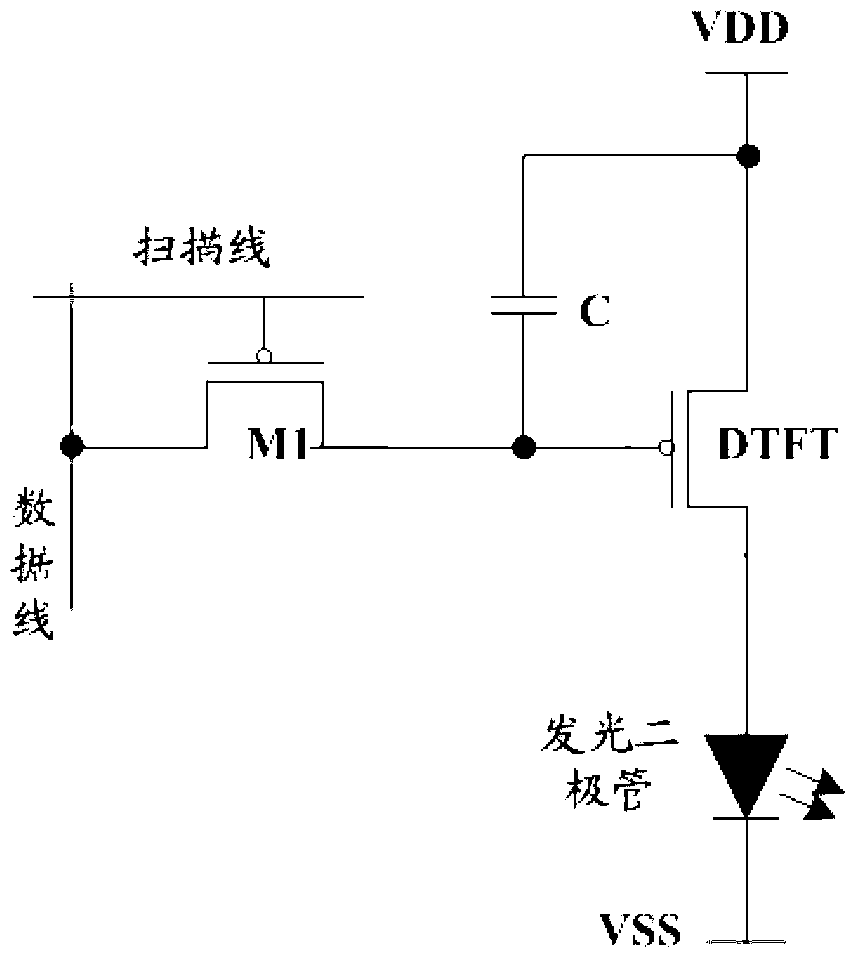
[0036] The embodiment of the present invention provides a light emitting diode pixel unit circuit and a display panel to solve the problem of uneven brightness of the display panel caused by different thresholds of thin film transistors.

[0037] The present invention will be described below with reference to the drawings.

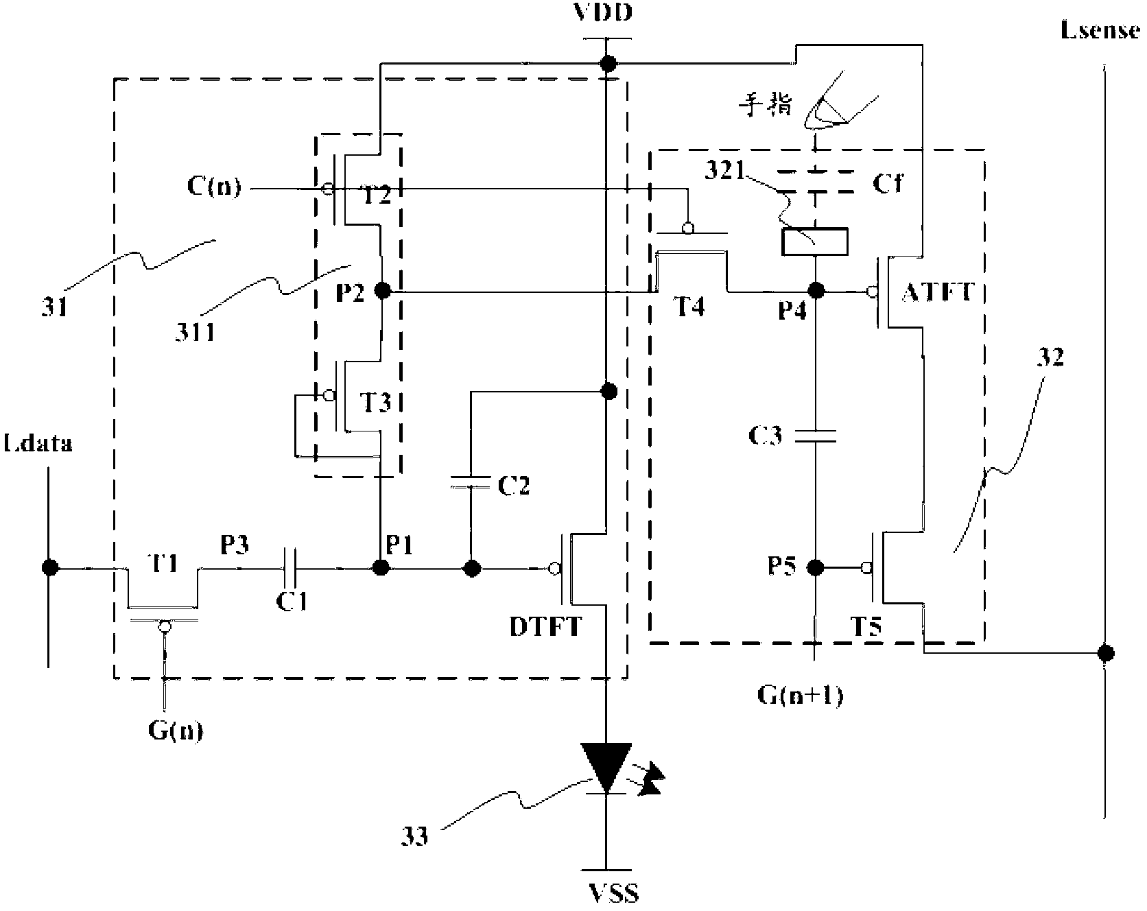
[0038] See image 3 , image 3 It is an active matrix active organic light emitting diode pixel unit circuit provided by an embodiment of the present invention, and the circuit includes: a driving module 31, a sensing module 32, and a light emitting diode 33;

[0039] Specifically, the driving module 31 includes: a driving thin film transistor DTFT, a first thin film transistor T1, a first capacitor C1, a second capacitor C2, and a driving control unit 311; wherein, the driving control unit 311 includes a second thin film transistor T2 And the third thin film transistor T3.

[0040] The gate of the driving thin film transistor DTFT is connected to the first node P...


PUM


Abstract

The invention provides a light emitting diode pixel unit circuit and a display panel to solve the problem that the display panel has nonuniform brightness because of different threshold voltages of thin film transistors; meanwhile, a touch screen circuit is integrated in the pixel unit circuit to realize the touch function of the light emitting diode display panel. The circuit comprises a driver module; the driver module comprises a driving thin film transistor, a first switch element, a first capacitor, a second capacitor and a drive control unit, wherein the drive control unit comprises a matching tube of which the threshold voltage is matched with that of the driving thin film transistor; the matching tube is positioned between the positive voltage output end of a power supply and a first node, and is used for saving the threshold voltage of the matching tube by controlling the charging and discharging of the second capacitor so as to compensate the threshold voltage of the driving thin film transistor.

Description

technical field [0001] The invention relates to the field of display technology, in particular to a light emitting diode pixel unit circuit and a display panel. Background technique [0002] Active Matrix Organic Light Emitting Diode (AMOLED, Active Matrix-Organic Light Emitting Diode) display panels have the characteristics of faster response speed, higher contrast ratio, and wider viewing angle than traditional liquid crystal panels. The pixels of the AMOLED display panel rely on the related drive circuit on the array (Array) substrate to drive the light-emitting display, see figure 1 , figure 1 It is a 2T1C pixel driving circuit in the prior art. From figure 1 It can be seen from the figure that the 2T1C pixel drive circuit in the prior art includes two thin-film transistors (TFT, Thin-Film Transistor) and a capacitor, wherein the thin-film transistor M1 acts as a switch for controlling the data line and the thin-film transistor DTFT The gate connection of the thin fi...

Claims


Application Information

Patent Timeline
IPC IPC(8): G09G3/32
CPCG06F3/0412G06F3/04184G06F3/044G09G3/3233G09G2300/0819G09G2300/0852G09G2310/0262G09G2320/0233G09G2320/043G09G3/2007G09G3/3266G09G2310/0251G09G2320/045G09G2354/00
Inventor 青海刚祁小敬
Owner BOE TECH GRP CO LTD
Why Eureka
Try Eureka