OLED (organic light emitting diode) pixel limit structure and manufacturing method thereof

A pixel-defining and pixel-defining layer technology, which is applied in semiconductor/solid-state device manufacturing, electrical components, diodes, etc., can solve the problems of increasing equipment investment, high cost, and affecting the luminous quality of the display backplane

Active Publication Date: 2013-09-18
BOE TECH GRP CO LTD
View PDF6 Cites 46 Cited by
  • Summary
  • Abstract
  • Description
  • Claims
  • Application Information

AI Technical Summary

Problems solved by technology

[0005] An embodiment of the present invention provides an OLED pixel-defining structure to solve the problem that when making a pixel-defining layer, since the size of the pixel-defining area is small, it is necessary to control the droplet to accura

Method used


Image

  • OLED (organic light emitting diode) pixel limit structure and manufacturing method thereof
  • OLED (organic light emitting diode) pixel limit structure and manufacturing method thereof
  • OLED (organic light emitting diode) pixel limit structure and manufacturing method thereof

Examples


Embodiment Construction

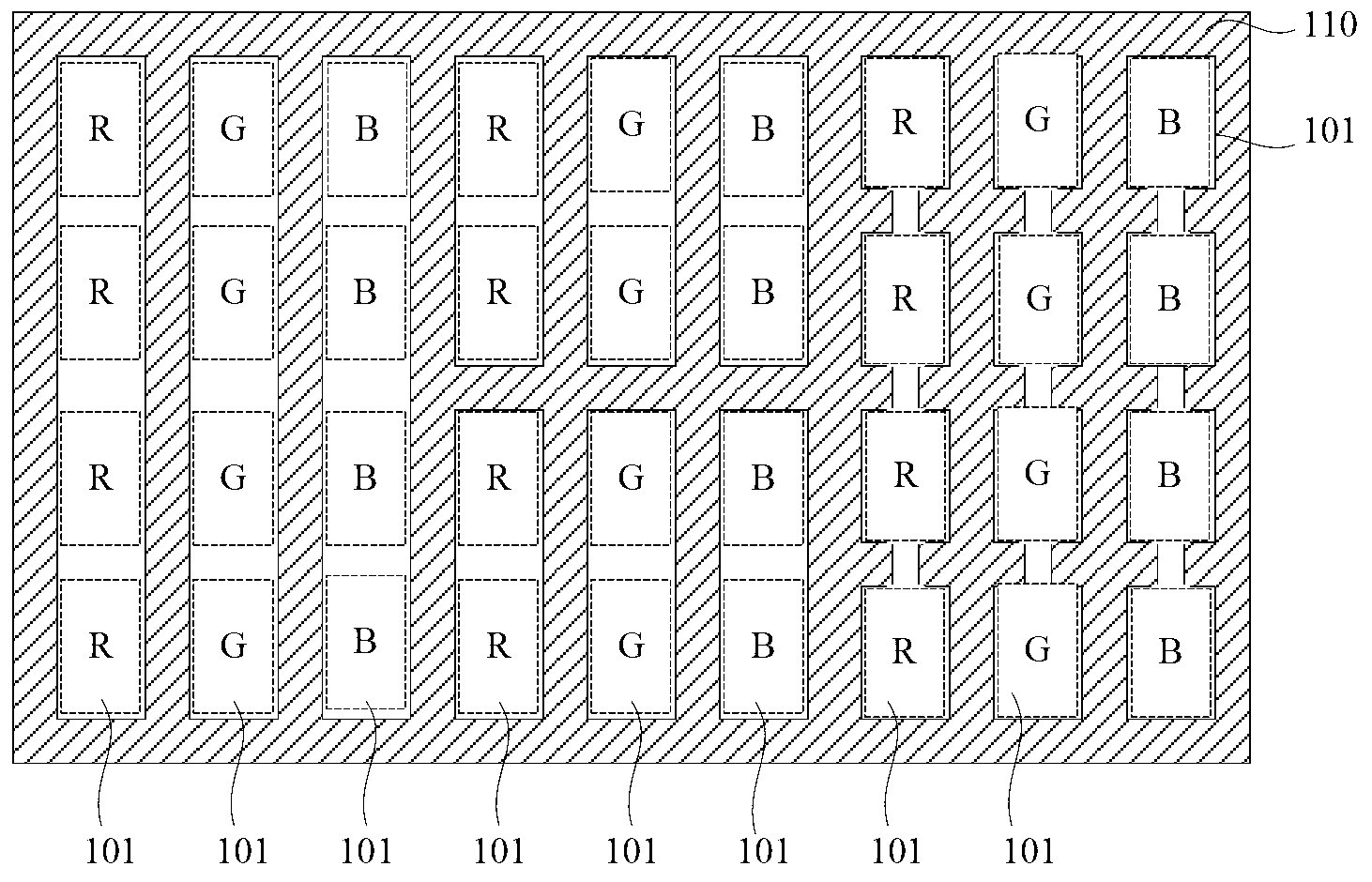
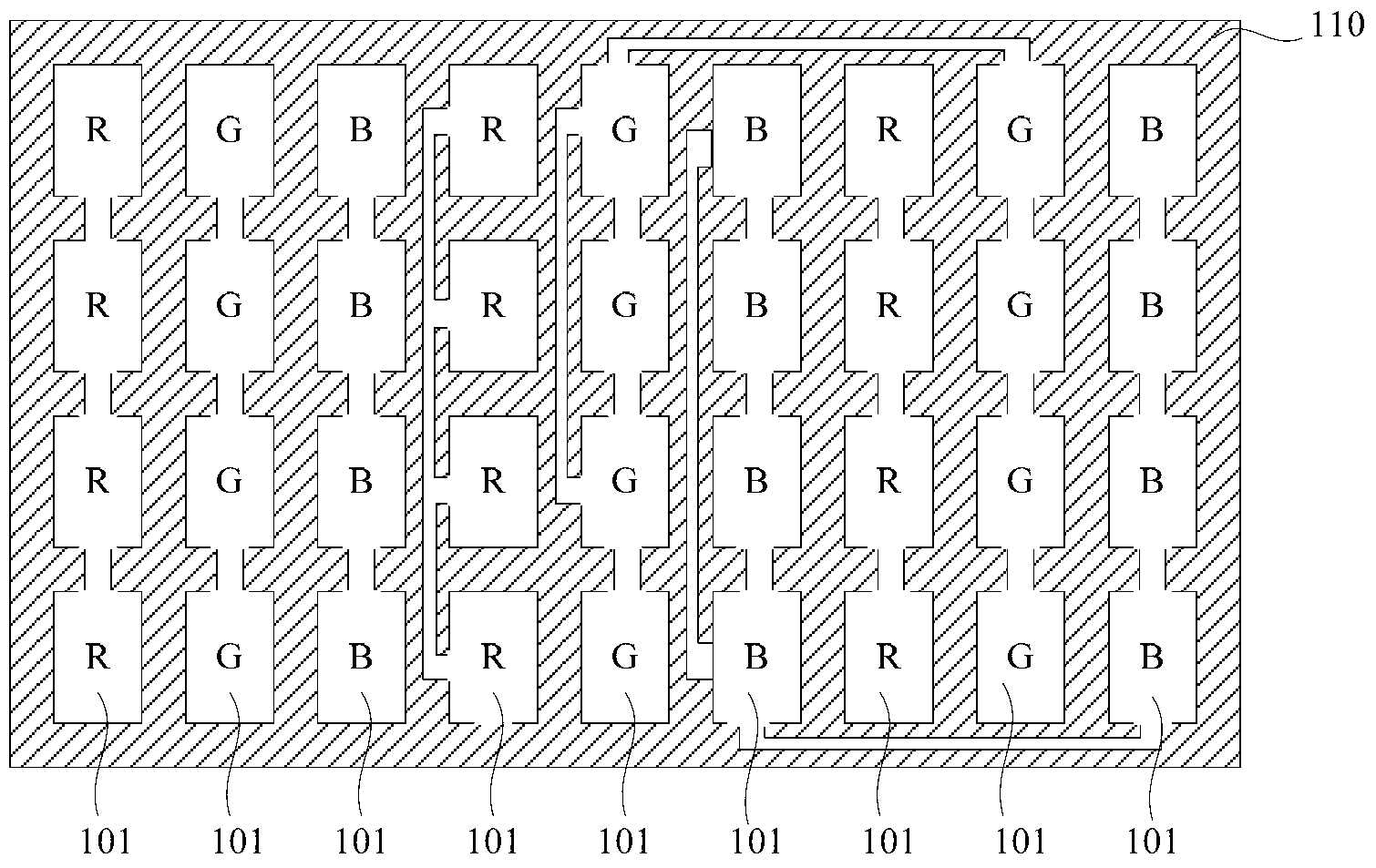
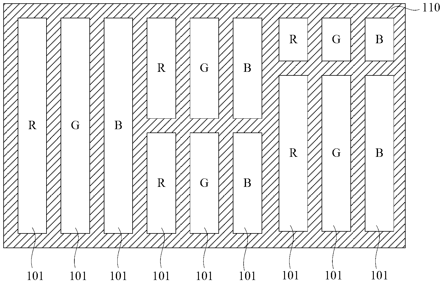
[0022] The OLED pixel definition structure in the embodiment of the present invention includes a pixel definition layer; the pixel definition layer includes sub-pixel definition regions of different colors, wherein at least two sub-pixel definition regions of the same color are connected; The at least two sub-pixel defined areas are connected, and the liquid droplets fall into the connected sub-pixel defined areas, and through the fluidity of the liquid, the connected sub-pixel defined areas are filled with liquid; and because at least two sub-pixel defined areas are connected, The fluidity of the liquid is increased, and it is easier to form a thin film with a uniform thickness in the sub-pixel limited area; thereby improving the luminous quality of the display backplane.

[0023] The embodiments of the present invention will be further described in detail below in conjunction with the accompanying drawings.

[0024] Such as figure 1 As shown, it is an OLED pixel definition ...


PUM


Abstract

The invention relates to the field of display, in particular to an OLED (organic light emitting diode) pixel limit structure and a manufacturing method thereof. The invention aims to solve the problems that during the manufacturing of a pixel definition layer, as the pixel definition size is smaller, and liquid drops need to be precisely controlled to fall to the pixel limit area, the equipment investment is increased, the higher cost is caused, and the pixel limit area is difficult in forming a film with uniform thickness. The pixel definition layer in the embodiment of the invention includes sub pixel limit areas of different colors, and at least two sub pixel limit areas with the same color are communicated with each other; at least two sub pixel limit areas with the same color of the pixel definition layer are communicated with each other, so liquid drops fall to the communicated sub pixel limit areas to enable the communicated sub pixel limit areas to be filled with liquid due to the liquidity of the liquid; at least two sub pixel limit areas are communicated, so that the liquidity of the liquid is increased, and the film with uniform thickness can be formed in the sub pixel areas more easily; and accordingly, the lighting quality of a back panel is improved.

Description

technical field [0001] The invention relates to the display field, in particular to an OLED pixel-defining structure and a manufacturing method thereof. Background technique [0002] Organic Light Emitting Diode (OLED) has unique characteristics such as self-illumination, fast response, wide viewing angle, and can be fabricated on flexible substrates. OLED-based displays are becoming the mainstream in the display field. [0003] The OLED display backplane includes a TFT substrate, an ITO (Indium Tin Oxide, indium tin oxide) pixel electrode, a light emitting layer, a cathode, and the like. A pixel defining layer is fabricated on the TFT substrate, and each pixel defining region corresponds to a pixel electrode. The smaller and denser each pixel defined area and the pixel electrodes corresponding to each pixel defined area are, the higher the resolution of the product will be. However, the finer pixel defined area is limited by printing technology. Taking the size of the pix...

Claims


Application Information

Patent Timeline
IPC IPC(8): H01L27/32H01L51/56
CPCH10K59/353H10K71/135H10K59/122H01L27/127H01L27/1292H01L21/0274H10K59/84H10K59/86H10K59/352H10K71/00H10K59/1201
Inventor 王辉锋刘则
Owner BOE TECH GRP CO LTD
Why Eureka
Try Eureka