Image sensor module with reduced overall thickness
An image sensing and image sensing element technology, applied in the field of image sensing modules, can solve the problems of reducing the overall thickness, the overall thickness cannot be effectively reduced, etc., and achieve the effect of reducing the overall thickness
- Summary
- Abstract
- Description
- Claims
- Application Information
AI Technical Summary
Problems solved by technology
Method used
Image

Examples
Embodiment 1
[0052] see Figure 2A to Figure 2D as shown, Figure 2A is a schematic top view of the flexible substrate before it is bent, Figure 2B for Figure 2A The schematic cross-section of 2B-2B, Figure 2C is a schematic side view of the flexible substrate before being bent, Figure 2D It is a schematic side view of the flexible substrate after being bent. It can be seen from the above figures that Embodiment 1 of the present invention provides an image sensing module Z with reduced overall thickness, which includes: a substrate unit 1 , a light-transmitting unit 2 , an image sensing unit 3 and a lens unit 4 .
[0053] First, cooperate Figure 2A and Figure 2B As shown, the substrate unit 1 includes at least one flexible substrate 10 , wherein the flexible substrate 10 has at least one through opening 100 . The light transmission unit 2 includes at least one light transmission element 20 disposed on the upper surface of the flexible substrate 10 and corresponding to the thro...
Embodiment 2
[0058] see image 3 As shown, Embodiment 2 of the present invention provides an image sensing module Z with reduced overall thickness, which includes: a substrate unit 1, a light-transmitting unit (not shown in the figure), an image sensing unit (not shown in the figure) and A lens unit 4 . Depend on image 3 and Figure 2A It can be seen from the comparison that the biggest difference between the second embodiment of the present invention and the first embodiment is: in the second embodiment, the substrate unit 1 includes a plurality of electronic components 11 arranged on the flexible substrate 10, and the plurality of electronic components 11 Two of them can be electrically connected to each other through a first conductive circuit W1 provided "simultaneously" on the main body 10A and one of the extension parts 10B. In other words, any two of the plurality of electronic components 11 of the present invention can be selectively passed through (1) "a first conductive line ...
Embodiment 3
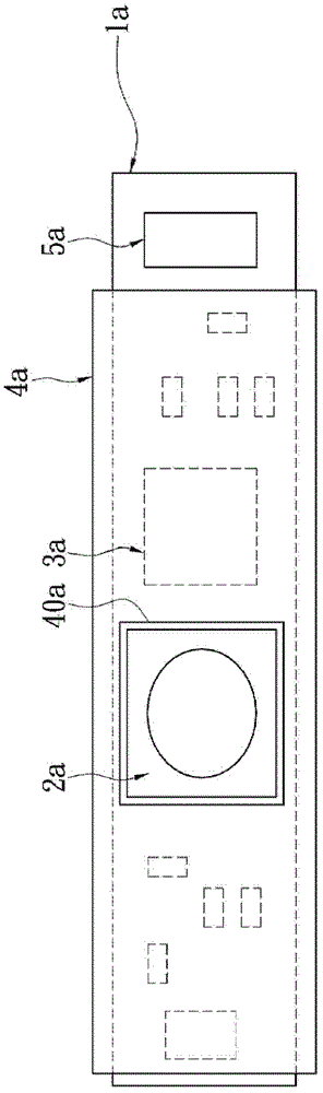
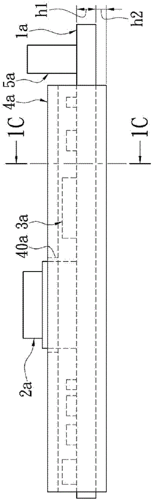
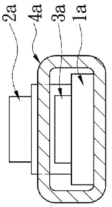
[0060] see Figure 4 As shown, the third embodiment of the present invention provides an image sensing module Z with reduced overall thickness, which includes: a substrate unit 1 , a light transmission unit 2 , an image sensing unit 3 and a lens unit 4 . The substrate unit 1 includes at least one flexible substrate 10 , wherein the flexible substrate 10 has at least one through opening 100 . The light transmission unit 2 includes at least one light transmission element 20 disposed on the upper surface of the flexible substrate 10 and corresponding to the through opening 100 . The image sensing unit 3 includes at least one image sensing element 30 disposed on the lower surface of the transparent element 20 and embedded in the through opening 100 , wherein the image sensing element 30 is electrically connected to the flexible substrate 10 . The lens unit 4 includes an opaque frame 40 disposed on the upper surface of the flexible substrate 10 and surrounding the transparent elem...
PUM
 Abstract
Description
Claims
Application Information
PatSnap Eureka turns technology decisions into work you can execute. Powered by our Innovation Knowledge Graph, it runs expert workflows across engineering, life sciences, materials and intellectual property. Get your review-ready output in minutes.


