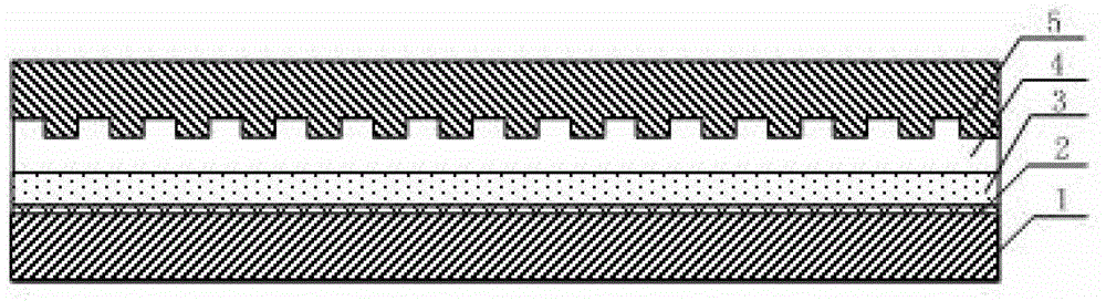
Preparation method of polyvinylidene fluoride with one-dimensional nanowire array structure
A nanowire array, polyvinylidene fluoride technology, applied in microstructure technology, microstructure device, manufacturing microstructure device and other directions, can solve the problems of inconvenient transfer and poor piezoelectric performance, and achieve no inconvenience in transfer and good pressure. The effect of electrical properties
- Summary
- Abstract
- Description
- Claims
- Application Information
AI Technical Summary
Problems solved by technology
Method used
Image

Examples
Embodiment 1
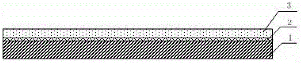
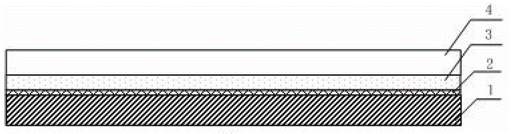
[0039] Step 1, prepare the metal electrode layer
[0040] Sputter a layer of SiO with a thickness of 350nm on the surface of a silicon substrate or a glass substrate 1 2 Make an insulating isolation layer 2, and then sputter a metal electrode layer 3 with a thickness of 100 nm on the surface of the insulating isolation layer 2;
[0041] Step 2, prepare polymer solution
[0042]In an environment with a temperature of 20°C, weigh 95% of dimethylformamide and 5% of acetone by volume percentage, and the sum of the volume percentages of the two is 100%. After mixing dimethylformamide and acetone , to prepare a mixed solution a; then dissolve the polyvinylidene fluoride powder or polyvinylidene fluoride copolymer powder in the mixed solution a to prepare a polymer solution, and the volume concentration of the polymer solution is 20 g / L;
[0043] Stir the polymer solution with a magnetic stirrer for 45 minutes, then place the polymer solution in a vacuum for 3 hours, and then seal ...
Embodiment 2
[0051] Step 1, prepare the metal electrode layer
[0052] Sputter a layer of SiO with a thickness of 200nm on the surface of silicon substrate or glass substrate 1 2 Make an insulating isolation layer 2, and then sputter a metal electrode layer 3 with a thickness of 300 nm on the surface of the insulating isolation layer 2;
[0053] Step 2, prepare polymer solution
[0054] In an environment with a temperature of 25°C, weigh 50% dimethylformamide and 5% acetone by volume percentage, and the sum of the volume percentages of the two is 100%. After mixing dimethylformamide and acetone , to prepare a mixed solution a; then dissolve the polyvinylidene fluoride powder or polyvinylidene fluoride copolymer powder in the mixed solution a to prepare a polymer solution, and the volume concentration of the polymer solution is 45 g / L;
[0055] Stir the polymer solution with a magnetic stirrer for 60 minutes, then place the polymer solution in vacuum for 2 hours, and then seal the polymer...
Embodiment 3
[0063] Step 1, prepare the metal electrode layer
[0064] Sputter a layer of SiO with a thickness of 500nm on the surface of a silicon substrate or a glass substrate 1 2 Make an insulating isolation layer 2, and then sputter a metal electrode layer 3 with a thickness of 500 nm on the surface of the insulating isolation layer 2;
[0065] Step 2, prepare polymer solution
[0066] In an environment with a temperature of 15°C, weigh 5% dimethylformamide and 95% acetone by volume percentage, and the sum of the two volume percentages is 100%. After mixing dimethylformamide and acetone , to prepare a mixed solution a; then dissolve the polyvinylidene fluoride powder or polyvinylidene fluoride copolymer powder in the mixed solution a to prepare a polymer solution, and the volume concentration of the polymer solution is 70 g / L;
[0067] Stir the polymer solution with a magnetic stirrer for 30 minutes, then place the polymer solution in a vacuum for 1 hour, and then seal the polymer s...
PUM
| Property | Measurement | Unit |
|---|---|---|
| thickness | aaaaa | aaaaa |
| thickness | aaaaa | aaaaa |
Abstract
Description
Claims
Application Information
 - R&D Engineer
- R&D Manager
- IP Professional
- Industry Leading Data Capabilities
- Powerful AI technology
- Patent DNA Extraction
Browse by: Latest US Patents, China's latest patents, Technical Efficacy Thesaurus, Application Domain, Technology Topic.
© 2024 PatSnap. All rights reserved.Legal|Privacy policy|Modern Slavery Act Transparency Statement|Sitemap