Magnetic resistance imaging sensor array

A magneto-resistive sensor and imaging sensor technology, applied to magnetic field controlled resistors, magnetic field measurement using electromagnetic devices, instruments, etc., to achieve improved resolution, less blind spots, and clear pictures

Active Publication Date: 2013-10-02
MULTIDIMENSION TECH CO LTD
View PDF13 Cites 11 Cited by
  • Summary
  • Abstract
  • Description
  • Claims
  • Application Information

AI Technical Summary

Problems solved by technology

[0009] However, none of these existing solutions disclose a high density multi-axis sensing full width scan head with an array capable of sensing both axes simultaneously

Method used


Image

  • Magnetic resistance imaging sensor array
  • Magnetic resistance imaging sensor array
  • Magnetic resistance imaging sensor array

Examples


Embodiment

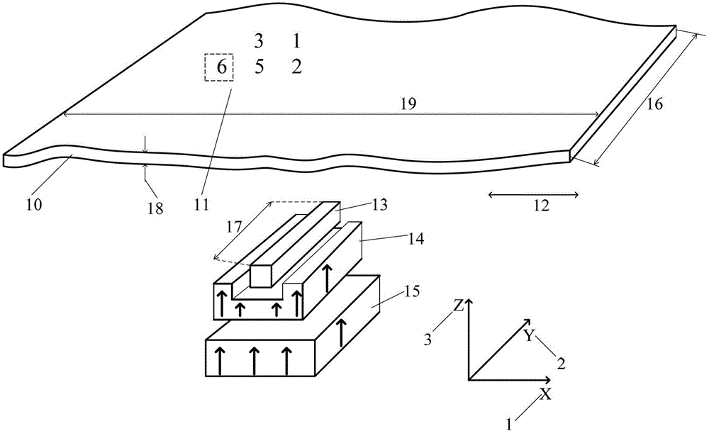
[0058] A magnetoresistance imaging sensor array for reading images from a medium, which includes a magnetic field excitation bias device of the medium, a magnetoresistance sensor chip, one or more electric excitation sources, a component selection circuit, and an output signal circuit. .

[0059] Such as Figure 5 As shown, the plane of the figure is parallel to the X-Y plane.

[0060] The magnetoresistive sensor chip is disposed between the magnetic field excitation bias device of the medium and the medium 10, which includes a main surface (namely X-Y plane) and a sensing surface 100, the sensing surface 100 is parallel to the main surface or in the X-Y plane.

[0061] The entire sensor array is 13 ratios Figure 5 The one shown in is even larger, and it is composed of several sub-chips 34, 34.1, 34.2, ..., 34.n arranged in rows / columns. The read width or the width of the medium is the same, that is, the width of the magnetoresistive sensor chip is the same as the readable...


PUM


Abstract

The invention relates to a magnetic resistance imaging sensor array which comprises a medium magnetic field stimulation and offset device, a magnetic resistance sensor chip, a plurality of magnetic resistance inducting elements, an electric excitation source, an element selecting circuit and an output signal circuit, wherein the magnetic resistance sensor chip comprises a main surface and an inducting surface, and an axis X and an axis Y which are perpendicular to each other are built in the main surface; the magnetic resistance inducting elements for forming an array are arranged in the inducting surface, one or more magnetic resistance inducting elements, of which the main inducting axes are parallel to the direction of the axis X, are X-axis inducting elements, and one or more magnetic resistance inducting elements, of which the main inducting axes are parallel to the direction of the axis Y, are Y-axis inducting elements; the electric excitation source is used for the excitation of the magnetic resistance inducting elements; the element selecting circuit is used for selecting the magnetic resistance inducting elements. The magnetic resistance imaging sensor array provided by the invention can be used for measuring magnetic field amplitude and magnetic field gradient in the axial direction, and the double-axis sensing capability enables pictures to be clearer and have fewer blind spots; the element selecting circuit can be used for monitoring absolute value and difference value of the magnetic field at any time and on any required time sequence.

Description

technical field [0001] The invention relates to the technical fields of banknote verification, magnetic reading head, imaging and the like, in particular to a magnetoresistance imaging sensor array used in the above fields. Background technique [0002] The maximum diameter of the physical area dotted at high resolution on the paper is 25 microns. An electronic image detector that reads an image from a medium and converts the image into an electrical signal, usually in digital data format, from which the image or data can be displayed on a screen or reproduced. [0003] Microprinting technology is mainly used in the following fields: banknote printing, copying, watermarking, paper document security. Sensing requirements in these areas vary as data can be in multiple formats eg magnetic ink, optical ink. In addition, there are almost no restrictions on the printing format. A printed word or object can be anywhere on the medium, can be of any shape, and can use any strength ...

Claims


Application Information

Patent Timeline
Patent Type & Authority Applications(China)
IPC IPC(8): G01R33/022G01R33/09
CPCG01R33/022G01R33/09H10N50/10
Inventor 薛松生詹姆斯·G·迪克金英西沈卫锋马克·C·仝大
Owner MULTIDIMENSION TECH CO LTD
Why Eureka
Try Eureka