Check patentability & draft patents in minutes with Patsnap Eureka AI!

Packaging structure

A technology of packaging structure and chip structure, which is applied in the direction of semiconductor/solid-state device parts, semiconductor devices, electrical components, etc., and can solve problems such as electromagnetic interference

Active Publication Date: 2013-10-23
NAN YA TECH
View PDF5 Cites 1 Cited by
  • Summary
  • Abstract
  • Description
  • Claims
  • Application Information

AI Technical Summary

Problems solved by technology

[0005] The invention provides a packaging structure to solve the defect of electromagnetic interference between different packaging structures

Method used


Image

  • Packaging structure
  • Packaging structure
  • Packaging structure

Examples


Embodiment Construction

[0026] Although the present invention is disclosed as follows with preferred embodiments, it is not intended to limit the present invention. Any person skilled in the art may make some changes and modifications without departing from the spirit and scope of the present invention. Therefore, the present invention The scope of protection is defined by the claims. In order not to obscure the spirit of the present invention, details of some known structures and process steps will not be disclosed here.

[0027] Likewise, the accompanying drawings represent schematic diagrams of devices in preferred embodiments, but are not intended to limit the size of the devices. In particular, to make the present invention more clearly presented, the sizes of some components may be enlarged in the drawings. Moreover, the same components disclosed in multiple preferred embodiments will be marked with the same or similar symbols to make the description easier and clearer.

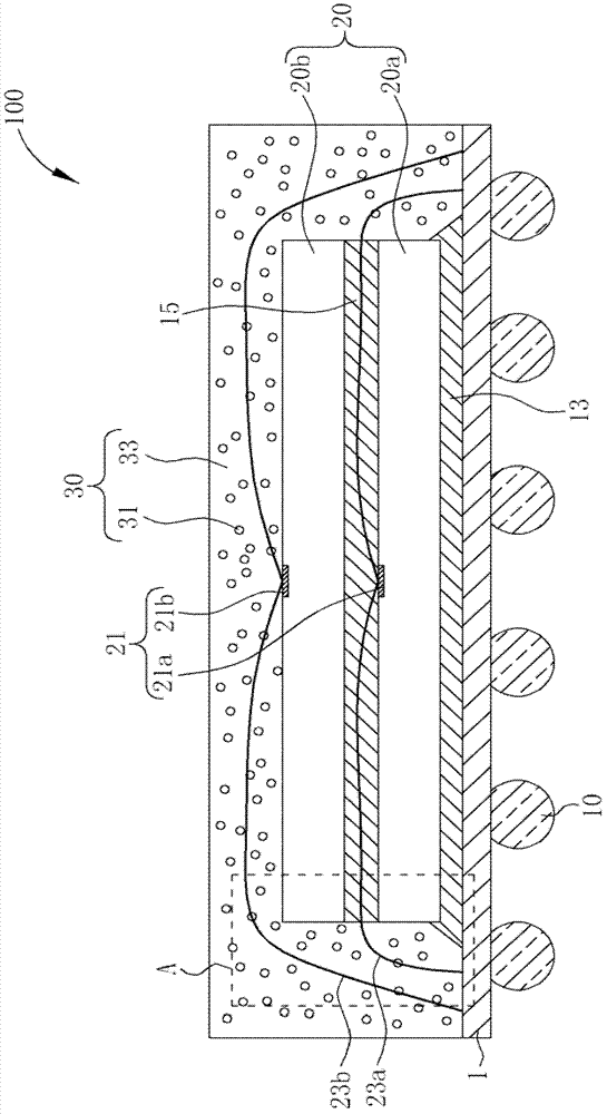
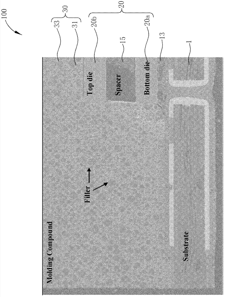
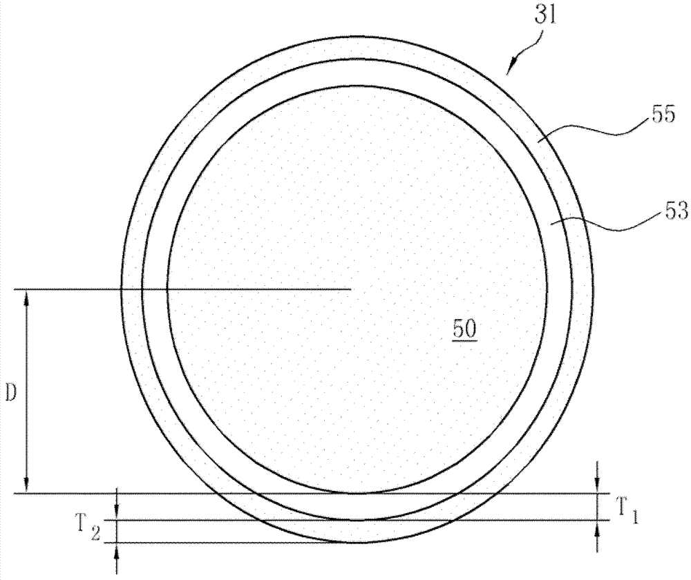
[0028] refer to figur...


PUM


Abstract

The invention discloses a packaging structure which comprises a carrier plate, at least one chip structure arranged on the carrier plate, a molding compound layer wrapping and directly contacting the chip structure, and a plurality of filler particles uniformly distributed in the molding compound layer, wherein each filler particle includes a dielectric core, an insulation layer wrapping the dielectric core, and a conductive layer arranged between the dielectric core and the insulation layer and forwardly wrapping the dielectric core.

Description

technical field [0001] The invention relates to a packaging structure, in particular to a packaging structure used for chip packaging. Background technique [0002] As we all know, packaging technology is actually to isolate the chip from the outside world to protect the chip circuit and avoid electrical performance degradation. On the other hand, the packaged chip is also easier to install and transport. The quality of the packaging technology also directly affects the performance of the chip itself The play and the design and manufacture of the PCB (printed circuit board) connected to it, so it is crucial. [0003] With the development of memory, the existing two-dimensional packaging technology is gradually replaced by three-dimensional packaging technology. The advantage of three-dimensional packaging is that it can increase the density of interconnect lines and reduce the package size (form factor). In the three-dimensional packaging of chip stacking, the chips are bon...

Claims


Application Information

Patent Timeline
Patent Type & Authority Applications(China)
IPC IPC(8): H01L23/552
CPCH01L2924/15311H01L2224/32145H01L2224/32225H01L2224/48227H01L2224/73265H01L2924/00
Inventor 陈逸男徐文吉叶绍文刘献文
Owner NAN YA TECH
Features
  • R&D
  • Intellectual Property
  • Life Sciences
  • Materials
  • Tech Scout
  • Unparalleled Data Quality
  • Higher Quality Content
  • 60% Fewer Hallucinations
Learn More