Printed circuit board
A technology of printed circuit boards and circuit boards, which is applied in the direction of printed circuit components, electrical connection printed components, etc., can solve the problems of high production testing costs and after-sales costs, unreliable connections, and poor reliability of printed circuit board products. Achieve the effects of low production inspection cost and after-sales cost, reliable connection, and reliable and stable connection
- Summary
- Abstract
- Description
- Claims
- Application Information
AI Technical Summary
Problems solved by technology
Method used
Image

Examples
Embodiment 1
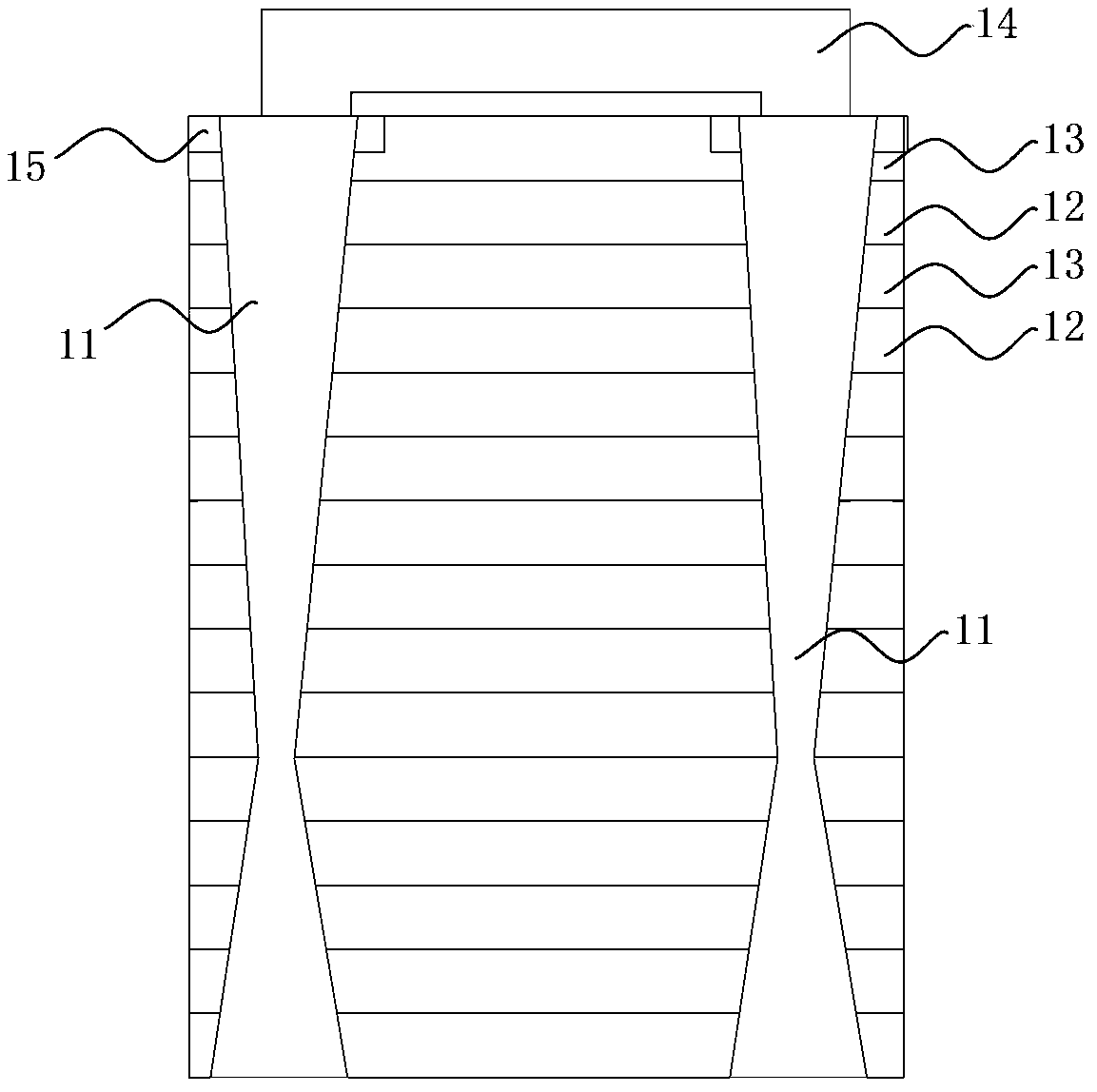
[0031] In this example, see figure 1 , a printed circuit board, which includes 8 layers of circuit boards, each layer of circuit boards includes a layer of substrate 12 and a layer of copper pads 13, the printed circuit board includes two for connecting printed circuit boards The via holes of all the circuit boards, that is, the via holes are through holes 11, and the shape of the through holes 11 is the shape presented when two tapered cone tops are butted. One end of the through hole 11 is connected to the component pad 15 of the electronic structural material 14 mounted on the printed circuit board.
[0032] The through hole 11 includes a conductive medium, the conductive medium has a larger contact area with each layer of the circuit board, and the conductive medium connects the component pad 15 so that the electronic structural material 14 is more firmly connected to the printed circuit board.
[0033] When the electronic structural material 14 is subjected to downward p...
Embodiment 2
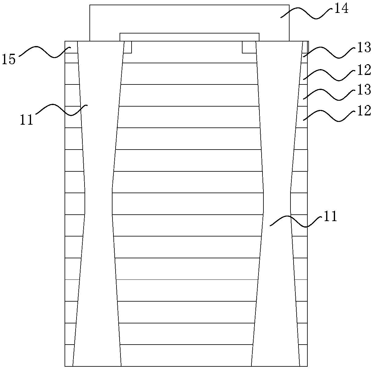
[0037] see figure 2 , this embodiment is basically the same as Embodiment 1, the only difference is that the shape of the through hole 11 is the shape presented when two tapered apexes are butted, and the shapes of the two tapered shapes are the same.
[0038] The shape of the through hole 11 is symmetrical, which is not only convenient to manufacture, but also more uniform when the force is applied, that is, the area of the force receiving surface is the same regardless of the downward force or the upward force. The connection between the printed circuit board and the electronic structural material 14 on it is more reliable.
Embodiment 3
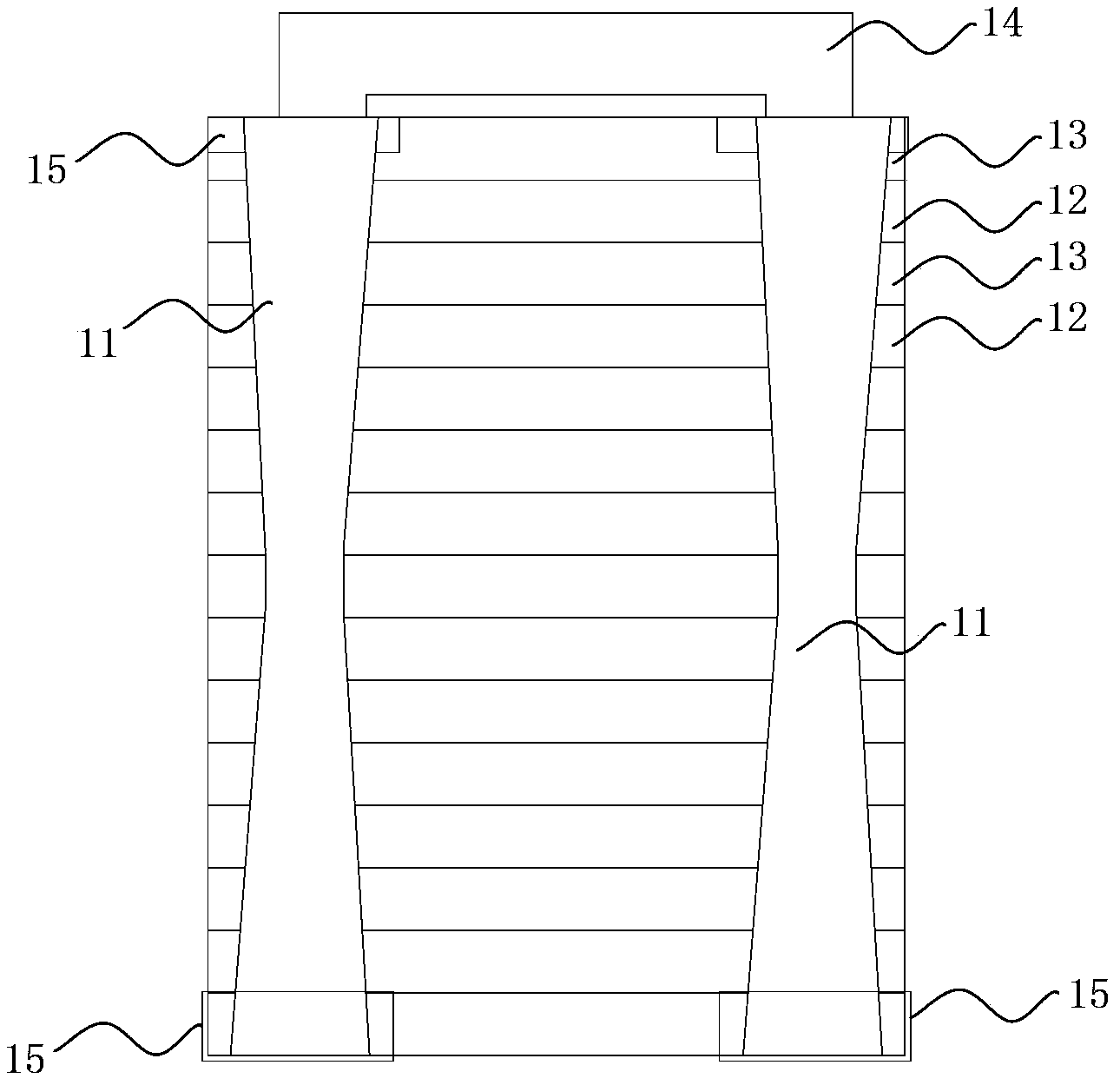
[0040] see image 3 , this embodiment is basically the same as Embodiment 2, except that both ends of the through hole 11 are connected to the component pads 15 of the electronic structural material 14 mounted on the printed circuit board. The through hole 11 connects two component pads 15 . Can meet the different needs of printed circuit boards.
PUM
 Abstract
Description
Claims
Application Information
 - R&D
- Intellectual Property
- Life Sciences
- Materials
- Tech Scout
- Unparalleled Data Quality
- Higher Quality Content
- 60% Fewer Hallucinations
Browse by: Latest US Patents, China's latest patents, Technical Efficacy Thesaurus, Application Domain, Technology Topic, Popular Technical Reports.
© 2025 PatSnap. All rights reserved.Legal|Privacy policy|Modern Slavery Act Transparency Statement|Sitemap|About US| Contact US: help@patsnap.com