Storage medium material, preparation method of storage medium material, and data storage method
- Summary
- Abstract
- Description
- Claims
- Application Information
AI Technical Summary
Problems solved by technology
Method used
Image

Examples
preparation example Construction
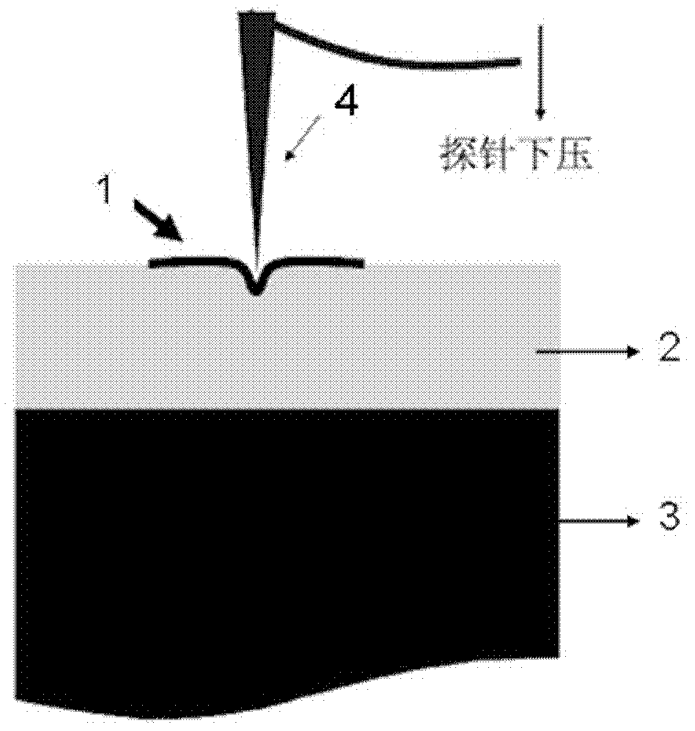
[0024] The preparation method of the storage medium material provided by the invention comprises sequentially forming a polymer layer and a graphite layer on a substrate, and the thickness of the graphite layer is not more than 10 nanometers, preferably 0.35-2 nanometers.
[0025] According to the present invention, the method for forming the polymer layer may be various existing methods, for example, may include coating a solution containing a polymer on a substrate and drying it. Generally speaking, the concentration of the polymer-containing solution can be 1-10% by volume, so that the solution can be more uniformly coated on the substrate. The polymer is used in an amount such that the thickness of the polymer layer is preferably 0.05-1 micron. The method of coating the solution containing the polymer on the substrate is well known to those skilled in the art, for example, methods such as spray coating, spin coating, flow coating, brush coating, and dipping can be used to ...
preparation example 1
[0040] This preparation example is used to illustrate the storage medium material and its preparation method provided by the present invention.
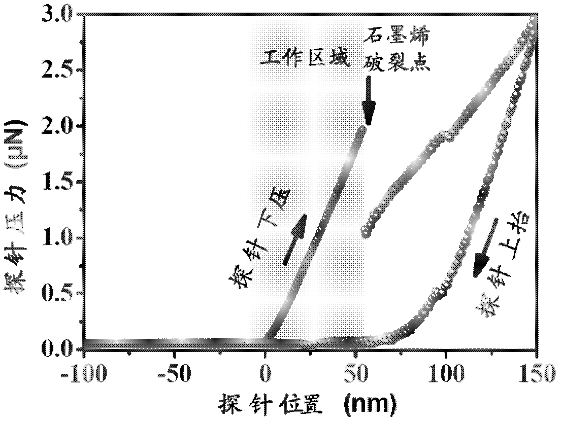
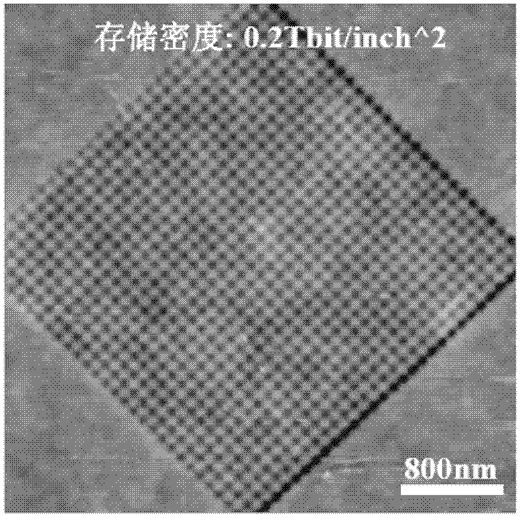
[0041] A silicon wafer with a thickness of 0.3 mm and a nano-level flat surface (purchased from SQI company, full name Silicon Quest International, Inc, the same below) was sequentially soaked in acetone, ethanol and deionized water for 10 minutes, and ultrasonically cleaned for 10 minutes. The frequency is 20kHz and the ultrasonic power is 800W. Spin-coat an acetone solution of polystyrene (Young's modulus 3GPa) with a concentration of 1% by volume on the treated substrate at a rotation speed of 800rpm, and dry at 150°C for 15 minutes to obtain a thickness of 0.05 Micron polymer layer. Use scotch tape to evenly stick the graphite powder, and stick the graphite powder side of the scotch tape to the polymer layer closely, remove the scotch tape, and use Raman spectroscopy to find a thickness of 0.35 nanometers on the polymer layer g...
preparation example 2
[0043] This preparation example is used to illustrate the storage medium material and its preparation method provided by the present invention.
[0044] A silicon nitride wafer (purchased from SQI company, full name Silicon Quest International, Inc) with a thickness of 1 mm and a nano-level flat surface was soaked in acetone, ethanol and deionized water for 10 minutes, and ultrasonic cleaning was performed for 10 minutes. 20KHz, ultrasonic power 800W. Concentration is 10 volume % polymethyl methacrylate (Young's modulus is 4GPa) acetone solution is spin-coated on the treated substrate, the rotating speed of spin-coating is 800rpm, and at 150 ℃, dry 15 minutes, obtain Polymer layer with a thickness of 1 micron. Use scotch tape to evenly stick the graphite powder, and stick the graphite powder side of the scotch tape to the polymer layer closely, remove the scotch tape, and use Raman spectroscopy to find a thickness of 2 nanometers on the polymer layer graphite layer, where, r...
PUM
| Property | Measurement | Unit |
|---|---|---|
| Thickness | aaaaa | aaaaa |
| Thickness | aaaaa | aaaaa |
| Thickness | aaaaa | aaaaa |
Abstract
Description
Claims
Application Information
 - R&D Engineer
- R&D Manager
- IP Professional
- Industry Leading Data Capabilities
- Powerful AI technology
- Patent DNA Extraction
Browse by: Latest US Patents, China's latest patents, Technical Efficacy Thesaurus, Application Domain, Technology Topic.
© 2024 PatSnap. All rights reserved.Legal|Privacy policy|Modern Slavery Act Transparency Statement|Sitemap