Light-emitting diode structure and method for manufacturing the same

A technology for light-emitting diodes and a manufacturing method, which is applied to electrical components, electrical solid-state devices, circuits, etc., can solve the problems of reducing the aspect ratio of the interconnection layer and the disconnection of the interconnection layer.

Inactive Publication Date: 2013-11-06
CHI MEI LIGHTING TECHNOLOGY CORP +1
View PDF6 Cites 4 Cited by
  • Summary
  • Abstract
  • Description
  • Claims
  • Application Information

AI Technical Summary

Problems solved by technology

Therefore, the aspect ratio of the interconnection layer can be greatly reduced, and the step coverage during deposition of the interconnection layer can be effectively improved, thereby solving the problem of disconnection of the interconnection layer

Method used


Image

  • Light-emitting diode structure and method for manufacturing the same
  • Light-emitting diode structure and method for manufacturing the same
  • Light-emitting diode structure and method for manufacturing the same

Examples


Embodiment Construction

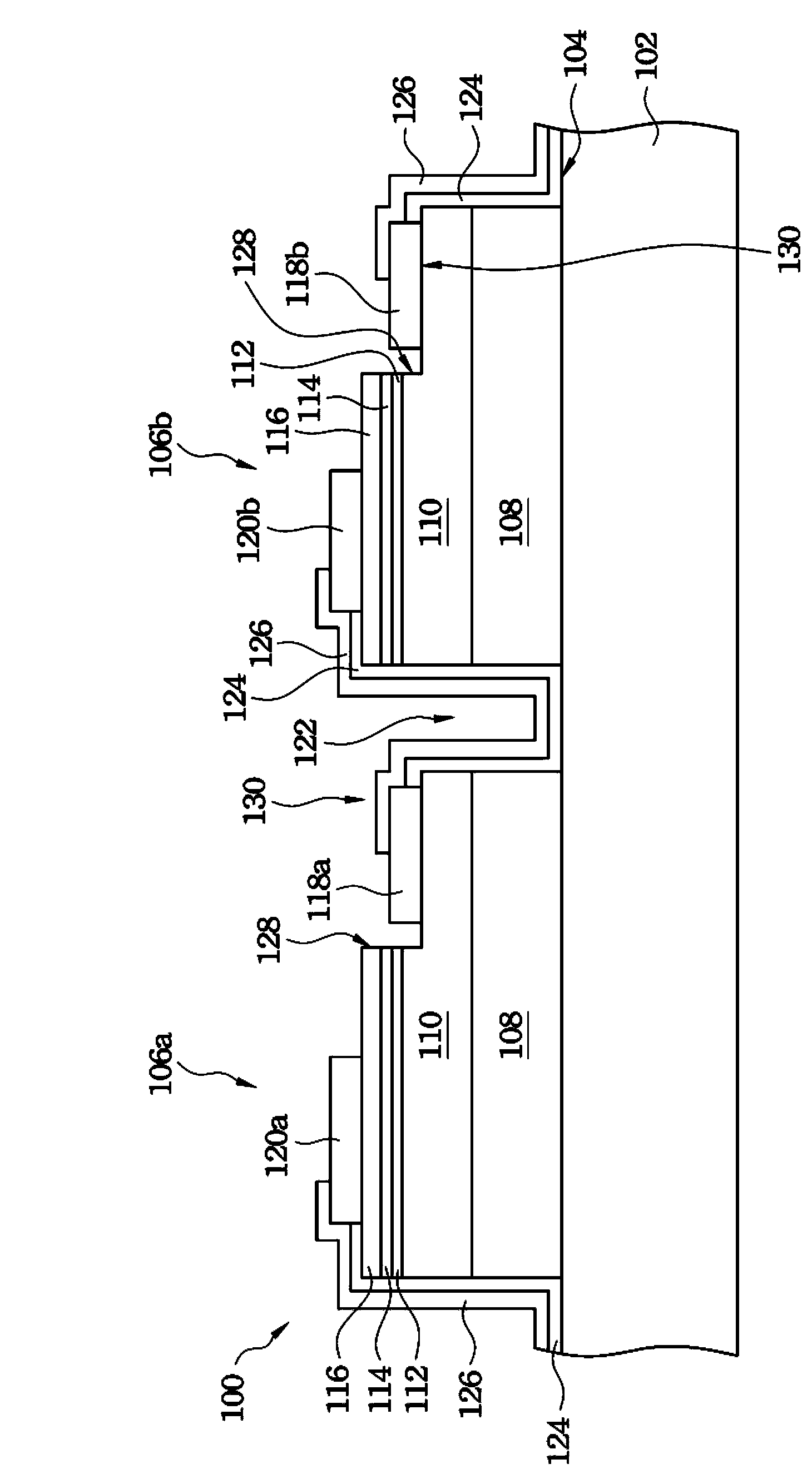
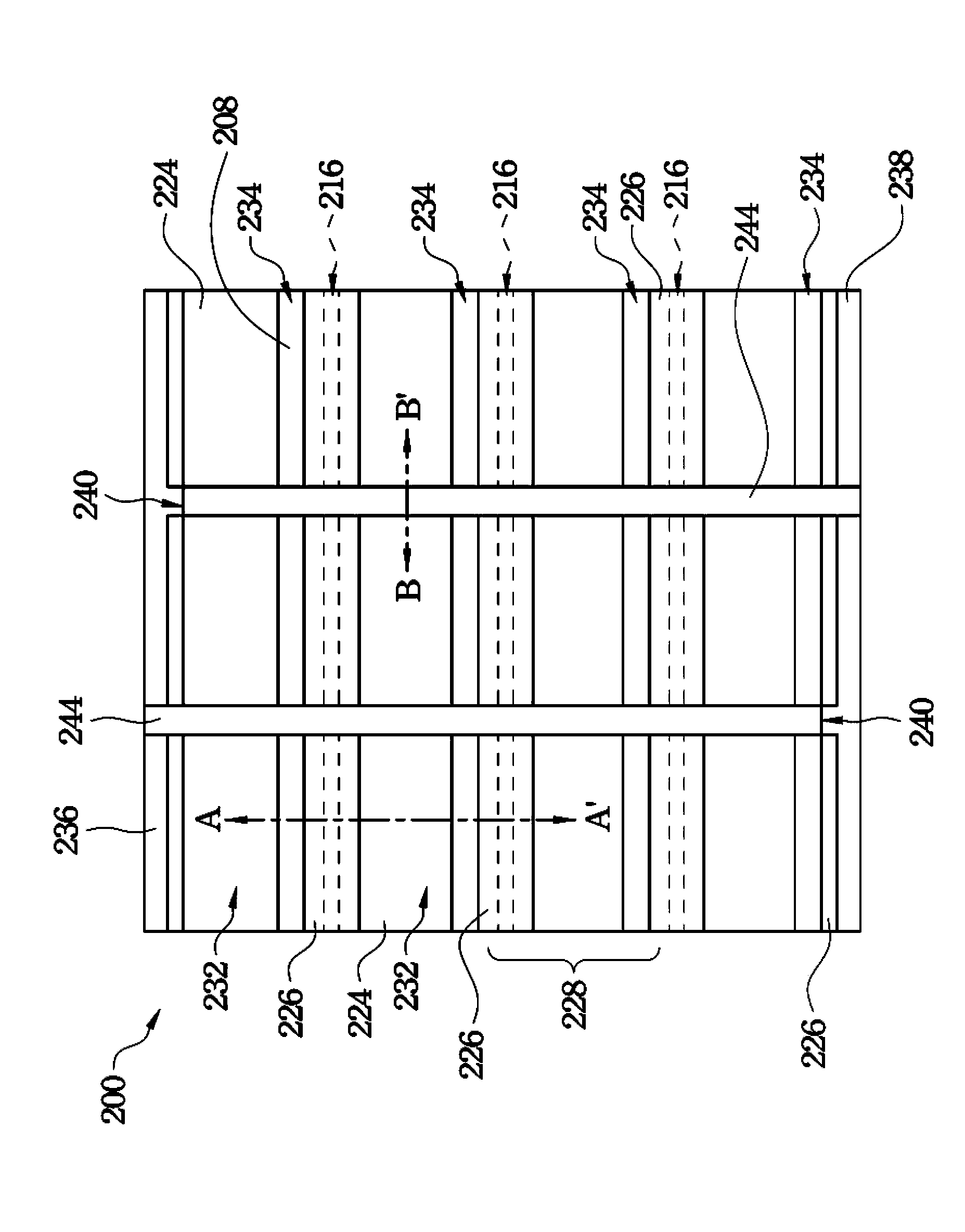
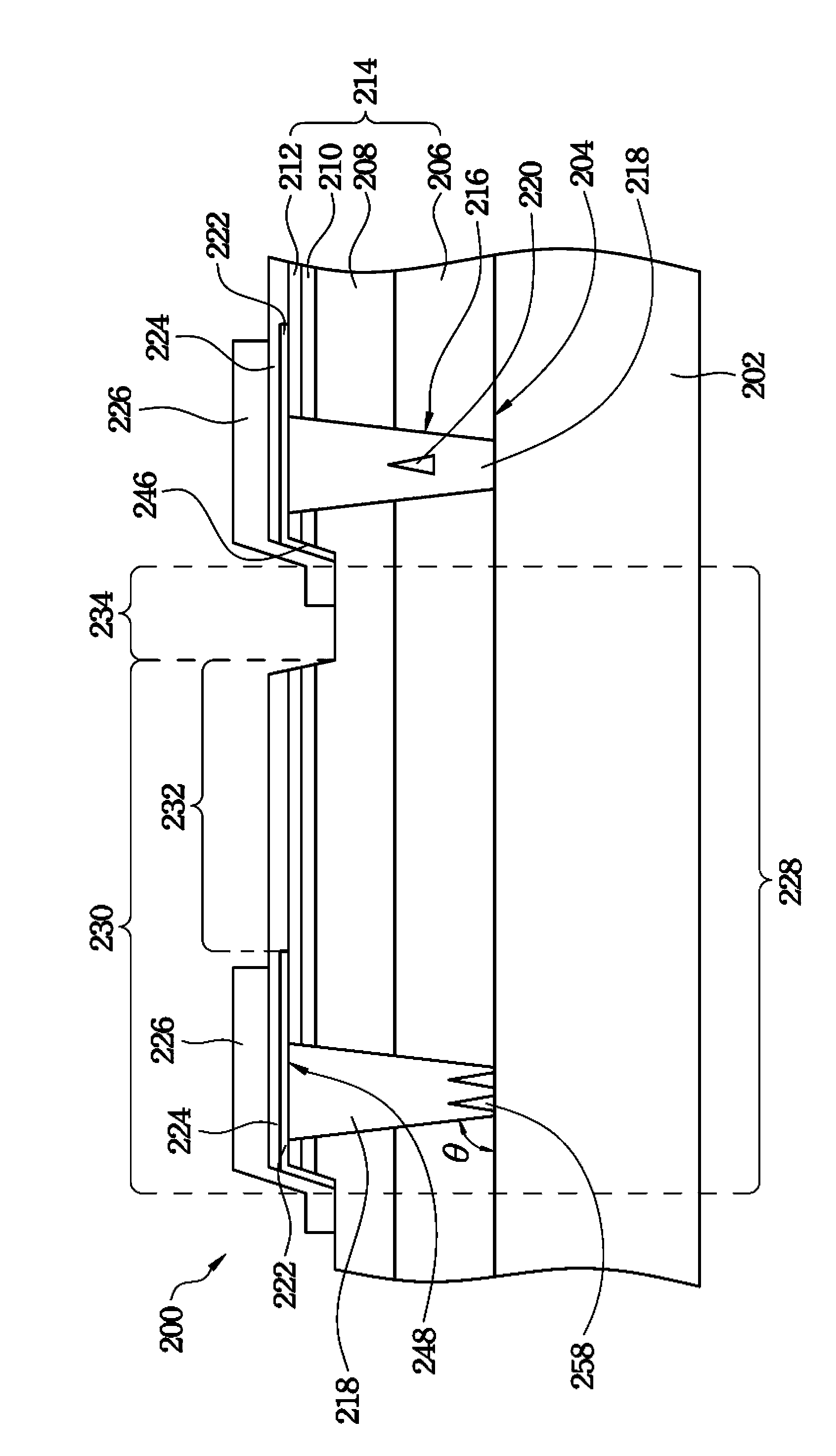
[0088] Please refer to Figure 2 to Figure 4 ,in figure 2 A top view showing a light emitting diode structure according to an embodiment of the present invention, Figure 3A drawn along figure 2 The cross-sectional view of the light-emitting diode structure obtained by the AA' section line, Figure 4 drawn along figure 2 The cross-sectional view of the LED structure obtained by the BB' section line. In this embodiment, the light emitting diode structure 200 may be a high voltage light emitting diode (High Voltage LED; HV LED).

[0089] like figure 2 As shown, the LED structure 200 is formed by connecting several LED chips 228 in series. exist figure 2 In the illustrated embodiment, the LED structure 200 is composed of 12 LED chips 228 connected in series. Isolation trenches 216 and 240 are provided around each LED chip 228 to electrically isolate these LED chips 228 . In addition, the adjacent LED chips 228 are electrically connected through the conductive interc...


PUM


Abstract

A light-emitting diode (LED) structure and a method for manufacturing the same. The LED structure comprises an insulating substrate, a plurality of LED chips (228) and a plurality of interconnection layers. Each LED chip comprises a first conductivity type semiconductor layer, an active layer and a second conductivity type semiconductor layer stacked in sequence on a surface of the insulating substrate. Each LED chip includes a mesa structure, an exposed portion of the first conductivity type semiconductor layer adjacent to the mesa structure, and a first isolation trench (216,240). The first isolation trench is disposed in the mesa structure. The interconnection layers (226) respectively connect neighboring two of the LED chips.

Description

technical field [0001] The present invention relates to a light emitting structure, and in particular to a light emitting diode (LED) structure and a manufacturing method thereof. Background technique [0002] Please refer to figure 1 , which shows a partial cross-sectional view of a conventional LED structure connected in series. The conventional series-connected LED structure 100 includes a plurality of series-connected LED chips, such as LED chips 106 a and 106 b , disposed on the surface 104 of an insulating substrate 102 . Two adjacent LED chips 106 a and 106 b are separated by an isolation trench 122 . Each LED chip 106a and 106b includes an undoped semiconductor layer 108, a first electrical type semiconductor layer 110, an active layer 112, a second electrical type semiconductor layer 114 and a transparent conductive layer stacked on the surface of the insulating substrate 102 in sequence. Layer 116. [0003] Each LED chip 106 a and 106 b has a mesa structure 128...

Claims


Application Information

Patent Timeline
Patent Type & Authority Applications(China)
IPC IPC(8): H01L27/15H01L33/00
CPCH01L27/153H01L33/20H01L33/62H01L2924/0002H01L2924/00H01L33/36
Inventor 朱长信李学麟徐智魁陈源泽
Owner CHI MEI LIGHTING TECHNOLOGY CORP
Why Eureka
Try Eureka