
power conversion device

A power conversion and source technology, applied in the direction of output power conversion devices, circuits, electrical components, etc., can solve the problems of insufficient BST node voltage, reduced circuit performance, and increased cost

Active Publication Date: 2016-05-25
HUAWEI TECH CO LTD
View PDF3 Cites 0 Cited by
  • Summary
  • Abstract
  • Description
  • Claims
  • Application Information

AI Technical Summary

Problems solved by technology

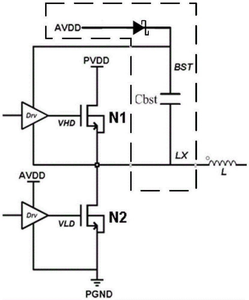
Another example figure 2 As shown, in phase1, AVDD is directly connected to the capacitor C through the Schottky diode BST Charging, but considering factors such as the forward conduction voltage drop of the Schottky diode (about 0.3 ~ 0.7V), the voltage of the BST node cannot be charged to AVDD, so in phase2, due to the continuity of the charge of the capacitor, the voltage of the BST node will be raised. As high as PVDD+AVDD-forward conduction voltage drop (0.3~0.7V), it may cause HighSideNMOS to be unable to conduct completely. For this reason, a minimum operating voltage of the circuit needs to be provided to offset the forward conduction voltage drop of the schottky diode
In addition, Schottky diodes have large reverse leakage, which degrades circuit performance
Again, if the BST circuit of the on-chip schottky diode is used, an additional Schottky process is introduced in the semiconductor process, which increases the process steps, increases the production cycle and cost accordingly, and limits the range of process options; External schottky diodes will increase the PCB board area and also increase the cost

Method used


Image

  • power conversion device
  • power conversion device
  • power conversion device

Examples


Embodiment Construction

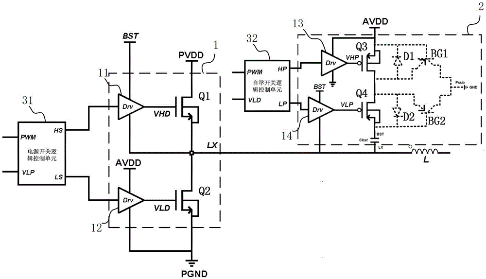
[0018] image 3 A power conversion device provided in the first embodiment of the present invention includes: a switch unit 1, a bootstrap unit 2 and a control unit 3.

[0019] The switch unit 1 includes: a first NMOS transistor Q1 and a second NMOS transistor Q2.

[0020] The first NMOS transistor Q1 is connected in series with the second NMOS transistor Q2, wherein the drain of the first NMOS transistor Q1 is connected to the power supply voltage PVDD, and the source is connected to the drain of the second NMOS transistor Q2, which is the power conversion device Output, the source of the second transistor Q2 is grounded.

[0021] The switch unit 1 further includes a first driving unit 11 and a second driving unit 12.

[0022] The signal input terminal of the first driving unit 11 is connected to an output of the power switch logic control unit 31 in the control unit 3, and the reference power terminal and the reference ground terminal are respectively connected to the two output ter...


PUM


Abstract

Embodiments of the present invention disclose a power supply conversion apparatus, where a control unit generates a corresponding control signal according to a received high level pulse width modulation signal, to control a first PMOS transistor Q3, a second PMOS transistor Q4, and a second NMOS transistor Q2 to be turned off successively, and then to make a first NMOS transistor Q1 conducted, which makes a voltage at a second end of a bootstrap capacitor to rise from ground potential to a PVDD, so that a voltage at a first end of the bootstrap capacitor rises to a PVDD+AVDD as the voltage at the second end rises, and a gate turn-on voltage of the first NMOS transistor Q1 reaches the PVDD+AVDD.

Description

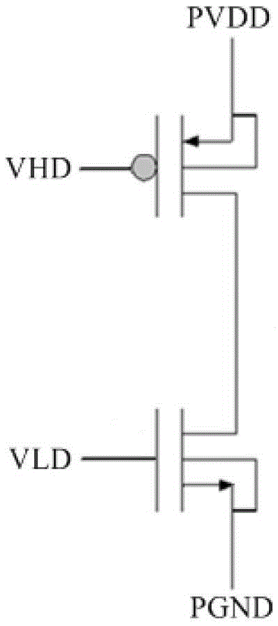
Technical field [0001] The present invention relates to the technical field of power switch circuits, in particular to a power conversion device. Background technique [0002] Mobile terminal products, such as mobile phones, portable instruments, notebook computers, etc., need to use a dedicated power management control chip to manage the charge and discharge of the device battery. Due to a series of considerations such as efficiency and heat dissipation, this type of power management chip gradually tends to adopt a switching mode with higher conversion efficiency and needs to work at a higher voltage (AC adapter input), so the chip generally needs to integrate one A switching DC-DC converter that can work under high input power supply voltage. When this converter is designed, there are big differences with different processes, especially its power output stage. For a process that supports high pressure, you can use such as figure 1 The traditional architecture of HighSidePMOS+...

Claims


Application Information

Patent Timeline
Patent Type & Authority Patents(China)
IPC IPC(8): H02M3/158H02M1/36
CPCH02M3/158H02M1/08H03K17/063H03K2217/0081
Inventor 李明王建平衡草飞
Owner HUAWEI TECH CO LTD
Learn More