A hybrid integrated circuit and its manufacturing method

A hybrid integrated circuit and manufacturing method technology, applied in circuits, semiconductor/solid-state device manufacturing, electrical components, etc., can solve problems such as difficulty and workload, damage to metallization layers, affect conductivity and corrosion resistance, etc. The effect of improving component performance, reducing placement difficulty, improving assembly operability and yield

Active Publication Date: 2016-01-20
CHINA ELECTRONIS TECH INSTR CO LTD
View PDF3 Cites 0 Cited by
  • Summary
  • Abstract
  • Description
  • Claims
  • Application Information

AI Technical Summary

Problems solved by technology

[0005] For transmission line circuits using soft dielectric substrates such as polytetrafluoroethylene, no matter whether they are bonded with epoxy resin or soldered with solder, when the circuit substrate is mounted, in order to ensure the flatness of the circuit after bonding or welding, the same shape will be used. The pressing block is pressed on the circuit substrate until the epoxy glue is cured or the solder is cooled. Therefore, there will be overflow of epoxy resin glue and solder in the MMIC chip integration groove, which needs to be removed to avoid affecting the mounting of the MMIC chip. It is difficult and labor-intensive to remove these spills, and the removal process will damage the metallization layer coated on the circuit carrier, affecting its conductivity and corrosion resistance

Method used


Image

  • A hybrid integrated circuit and its manufacturing method
  • A hybrid integrated circuit and its manufacturing method
  • A hybrid integrated circuit and its manufacturing method

Examples


Embodiment Construction

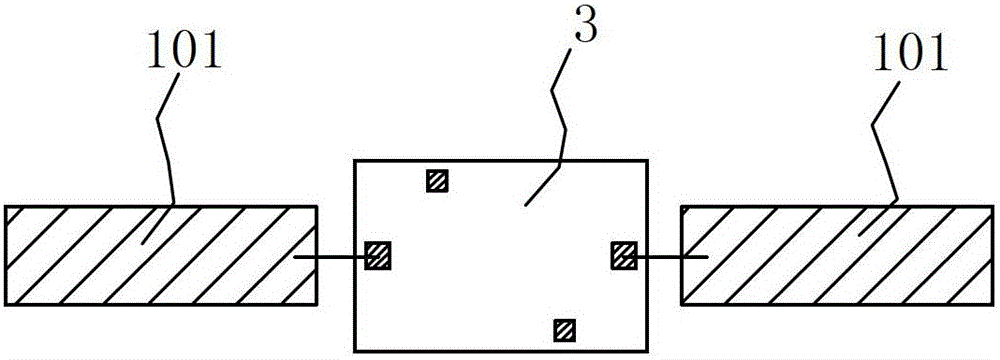
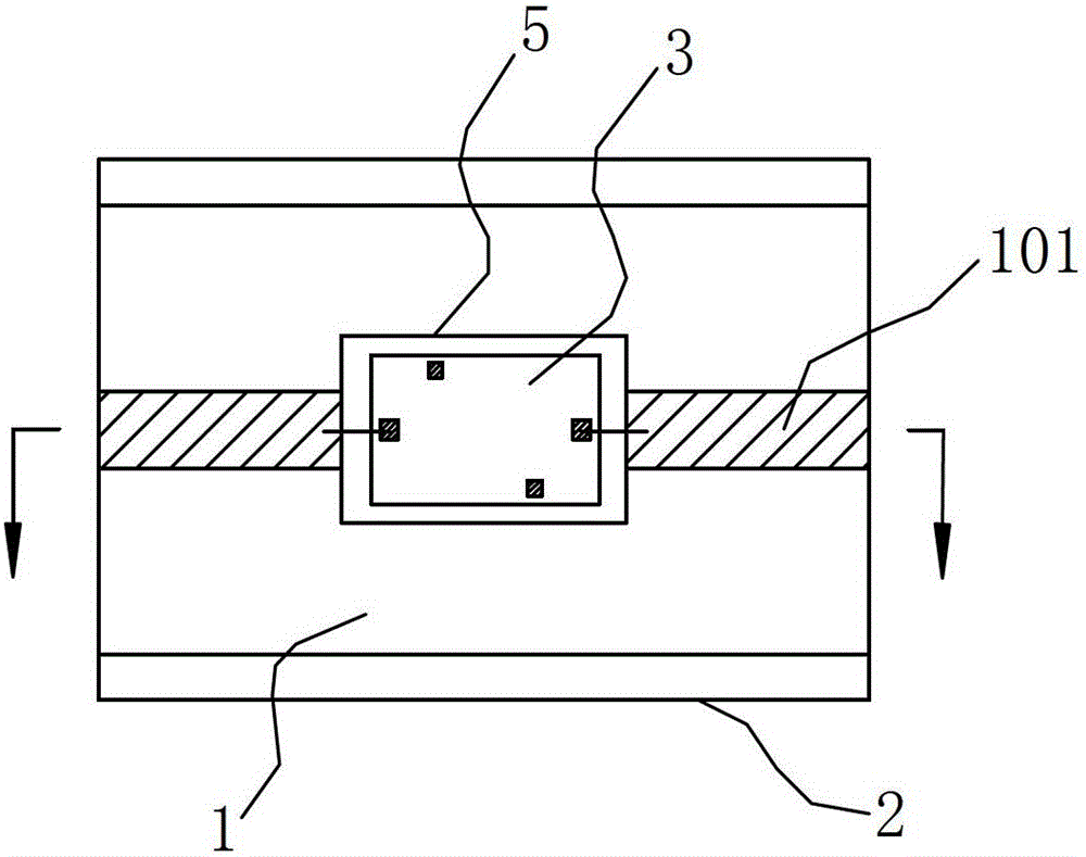
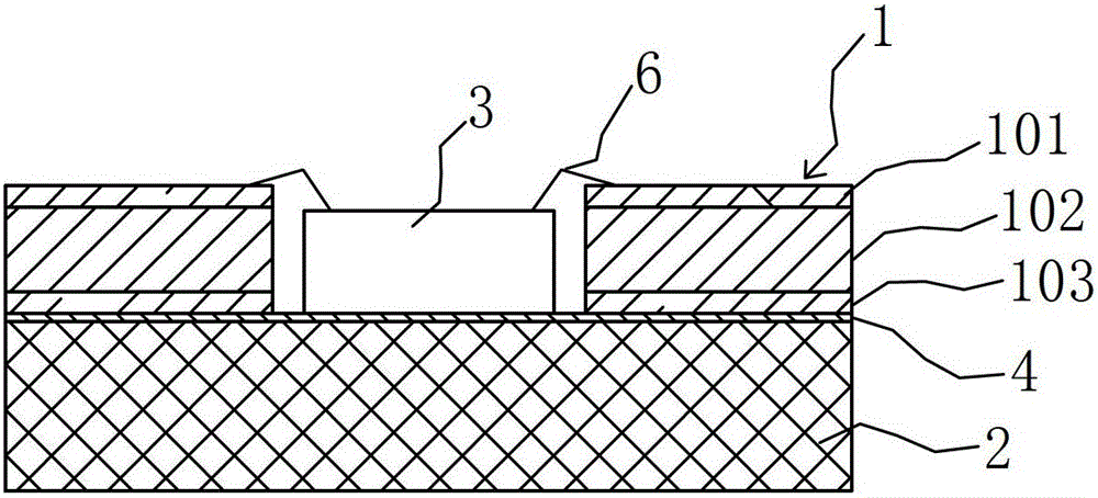
[0045] The present invention is based on the manufacturing technology of polytetrafluoroethylene soft dielectric circuits commonly used in hybrid integrated circuits, improves the processing form of the MMIC chip integration groove 5 in the traditional circuit, and processes the MMIC chip integration groove 5 into a blind groove 10 form , retaining the ground metal layer 103 on the original polytetrafluoroethylene circuit substrate, thereby reducing the bonding or welding difficulty of the MMIC chip 3, and improving the yield and reliability.

[0046] The specific solutions adopted by the present invention will be described in detail below in conjunction with the accompanying drawings.

[0047] combine Figure 6-Figure 21 ,in Figure 6-Figure 15 It shows the structural change diagram of the polytetrafluoroethylene copper clad laminate during the processing of the circuit substrate; Figure 16-Figure 21 A schematic diagram showing the structure of each stage in the hybrid int...


PUM


Abstract

The invention discloses a hybrid integrated circuit comprising a circuit carrier, a circuit substrate, an MMIC chip and a metal wire. The circuit substrate is provided with a blind groove. The MMIC chip is mounted in the blind groove. The circuit substrate and the MMIC chip are in bonding interconnection through the metal wire. The circuit substrate is bound on the circuit carrier by using a conductive epoxy resin adhesive or is welded on the circuit carrier by using a soldering material. According to the circuit, the integrated groove in the MMIC chip is the blind groove, the entering of the overflow when the circuit substrate is bound by using the conductive epoxy resin adhesive or is welded by using the soldering material can be effectively blocked, the pasting difficulty of the MMIC chip is decreased, the assembly operability and the rate of finished product of a component are raised, and the performance of component is improved.

Description

technical field [0001] The invention relates to a microwave and millimeter wave hybrid integrated circuit, and also relates to a manufacturing method of the hybrid integrated circuit. Background technique [0002] Many microwave and millimeter-wave hybrid integrated circuits use the assembly form of circuit substrate conduction band metal layer-MMIC chip-circuit substrate conduction band metal layer in series, and use metal wire or metal ribbon bonding in the middle to realize electrical interconnection, such as figure 1 shown. [0003] Both the circuit substrate and the MMIC chip are bonded with conductive epoxy resin or soldered to the circuit carrier. The circuit carrier is the mechanical support, electrical performance channel and heat dissipation channel of the circuit substrate and the MMIC chip. The circuit substrate Materials such as gold wire, aluminum wire or gold tape are used between MMIC chips, and ultrasonic (hot) pressure welding and bonding equipment are use...

Claims


Application Information

Patent Timeline
Patent Type & Authority Patents(China)
IPC IPC(8): H01L25/00H01L23/06H01L25/16H01L21/50
CPCH01L2224/05554H01L2224/48091H01L2224/48227H01L2924/00014
Inventor 王斌路波胡莹璐
Owner CHINA ELECTRONIS TECH INSTR CO LTD
Why Eureka
Try Eureka