Display device and pixel circuit thereof

A pixel circuit and electrode technology, which is applied in the field of display devices, can solve problems such as data writing and threshold compensation influence, complex circuit structure, complex pixel circuit, etc., and achieve the effect of solving threshold voltage drift

Active Publication Date: 2013-12-11
PEKING UNIV SHENZHEN GRADUATE SCHOOL
View PDF7 Cites 87 Cited by
  • Summary
  • Abstract
  • Description
  • Claims
  • Application Information

AI Technical Summary

Problems solved by technology

However, many voltage-driven pixel circuits require a complex circuit structure and introduce multiple gate drive circuit modules when compensating for threshold voltage drift, making the pixel circuit too complex and increasing the circuit cost
[0008] In addition, pixel circuits generally include two types of progressive scanning and simultaneous light-emitting types. For progressive scanning pixel circuits, when used in 3D display, in order to avoid crosstalk between left and right eye images, the scanning frequency needs to be increased to 480Hz. High scanning frequency makes data writing and threshold compensation affected
[0009] In addition, when the traditional progressive scan pixel circuit is used for 3D display, in order to avoid crosstalk between the left and right eye images, the scanning frequency needs to be increased to 480Hz, such a high scanning frequency will cause certain problems for data writing and threshold compensation. influences

Method used


Image

  • Display device and pixel circuit thereof
  • Display device and pixel circuit thereof
  • Display device and pixel circuit thereof

Examples


Embodiment 1

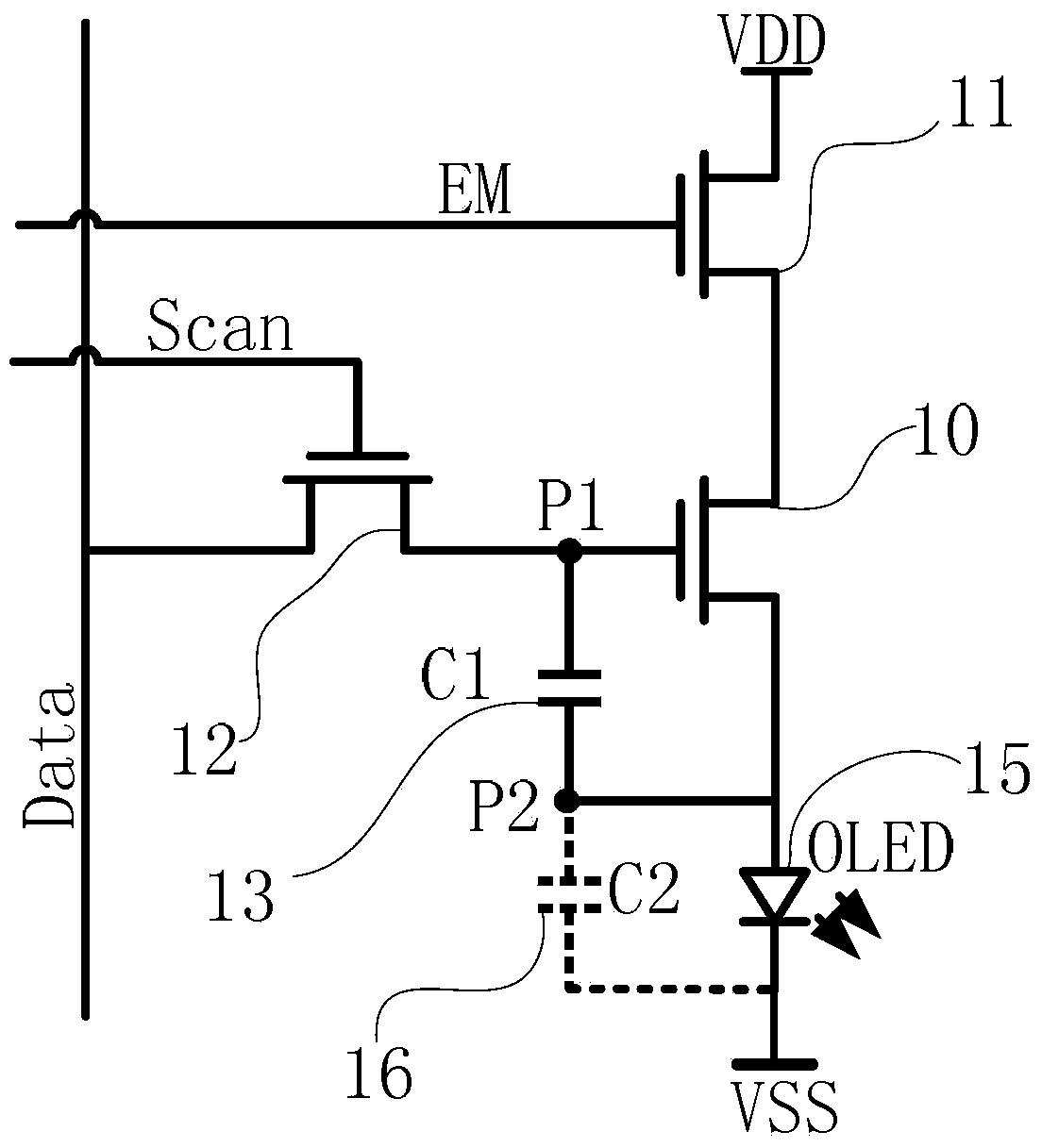
[0047] Please refer to image 3 , this embodiment provides a pixel circuit, including an OLED 15 , a driving transistor 10 , a storage capacitor 13 , a first switching transistor 12 and a second switching transistor 11 .

[0048] The driving transistor 10 includes a gate, a source and a drain, and the drain of the driving transistor 10 is coupled to the OLED 15 for providing driving current to the OLED 15 .

[0049] The first end of the storage capacitor 13 is connected to the gate of the driving transistor 10 , and the second end is connected to the drain of the driving transistor 10 .

[0050] The first switching transistor 11 is coupled between a power supply control line VDD and the source of the drive transistor 10, and the gate of the first switching transistor 11 is coupled to an emission control line EM; The signal provided by the control line VDD and the light emission control line EM, the first switch transistor 11 is turned on, and the turned on first switch transi...

Embodiment 2

[0072] Please refer to Figure 5 The difference between this embodiment and the first embodiment is that the transistors in the pixel circuit are P-type transistors.

[0073] Wherein, in the initialization phase, the first switching transistor 21 outputs the initialization level of the power control line VDD to the connection node P1 in response to the low level of the light emission control line EM, and the initialization level is a high level VH; threshold compensation after the initialization phase stage, the second switching transistor 22 outputs the reference level of the data line to the connection node P1 in response to the low level of the scanning line Scan, and the first switching transistor 21 is turned on in response to the low level of the light emission control line EM, and the connection node P2 is turned on. Discharge, and store the threshold voltage information of the driving transistor 20 at the connection node P2; in the data writing phase after the threshol...

Embodiment 3

[0078] Please refer to Figure 7 The difference between this embodiment and Embodiment 1 is that the pixel circuit provided by this embodiment further includes a third transistor 34, and the third transistor 34 is coupled between the data line Data and the drain of the driving transistor 30, and the third transistor 34 The gate is coupled to an initialization control line Ini for providing an initialization potential to the drain of the driving transistor 30 during the initialization phase of each frame scanning.

[0079] In this embodiment, the transistor of the pixel circuit is an N-type transistor, and in the initialization stage, the third transistor 34 responds to the high level of the initialization control line Ini to output the initialization level of the data line to the connection node P2, and the initialization level is a low level VL: In the threshold compensation stage after the initialization stage, the second switch transistor 32 outputs the reference level of t...


PUM


Abstract

Disclosed are a display device and a pixel circuit of the display device. According to a first switch transistor, in a threshold value compensation phase, signals provided by a power source control line and a light-emitting control line are responded to. The first switch transistor is switched on, and threshold value voltage information of a driving transistor is stored in a connecting node of a second electrode of the driving transistor and a light-emitting component. According to a second switch transistor, in a data writing-in phase, the first switch transistor is switched off, the second switch transistor is switched on by responding to a signal provided by a scanning line, and a data voltage provided by a data line is stored at a connecting node of the first end of a storage capacitor and a control electrode of the driving transistor. The compensation of threshold value voltage drifting of a TFT device and the light-emitting component is achieved, and the problem of uneven display caused by the threshold value voltage drifting of the driving transistor and the threshold value voltage of the light-emitting component is solved.

Description

technical field [0001] The present application relates to a display device, and in particular to a pixel circuit for the display device. Background technique [0002] Organic Light-Emitting Diode (OLED) display has been extensively studied in recent years due to its advantages of high brightness, high luminous efficiency, wide viewing angle and low power consumption, and has been rapidly applied to a new generation of displays. There are two driving modes for OLED display: passive matrix driving (Passive Matrix OLED, PMOLED) and active matrix driving (Active Matrix OLED, AMOLED). Although the cost of passive matrix driving is low, it cannot realize high-resolution display due to crosstalk phenomenon, and the passive matrix driving current is large, which reduces the service life of OLED. In contrast, the active matrix driving method sets a different number of transistors on each pixel as a current source, which avoids crosstalk, requires less driving current, and lower powe...

Claims


Application Information

Patent Timeline
Patent Type & Authority Applications(China)
IPC IPC(8): G09G3/32G09G3/3258G09G3/3266G09G3/3291
Inventor 张盛东冷传利蔡玉莹
Owner PEKING UNIV SHENZHEN GRADUATE SCHOOL
Why Eureka
Try Eureka