Shift register circuit

A technology of shift register circuit and shift register, which is applied in the direction of information storage, static memory, digital memory information, etc., can solve the problems of high cost, complex circuit design, and large circuit size, and achieve low cost, simple circuit design, The effect of small circuit size

Active Publication Date: 2013-12-18
AU OPTRONICS CORP
View PDF7 Cites 3 Cited by
  • Summary
  • Abstract
  • Description
  • Claims
  • Application Information

AI Technical Summary

Problems solved by technology

[0003] However, since each circuit stage in the known shift register circuit requires at least fifty transistors for circuit d

Method used


Image

  • Shift register circuit
  • Shift register circuit
  • Shift register circuit

Examples


Embodiment Construction

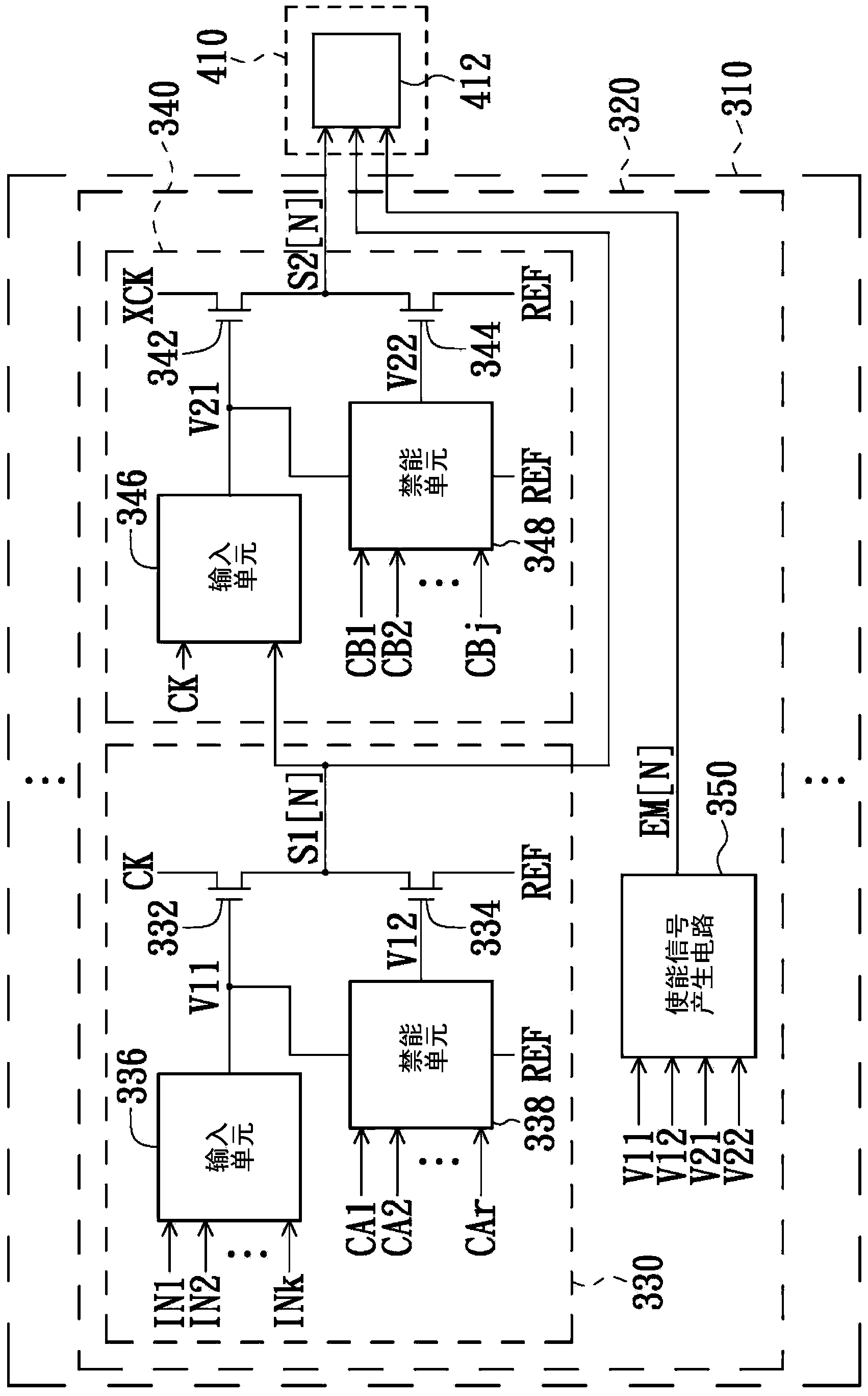
[0045] image 3 A shift register circuit according to an embodiment of the present invention is shown. Please refer to image 3 , and the symbol 310 represents the above-mentioned shift register circuit. The shift register circuit 310 is suitable for driving the organic light emitting diode display panel 410 . The shift register circuit 310 includes a plurality of circuit stages 320 connected in series, and each circuit stage 320 includes a first shift register 330 , a second shift register 340 and an enable signal generating circuit 350 . For the convenience of explanation, in the following description, it is assumed that image 3 The circuit stage 320 shown is the Nth circuit stage in the shift register circuit 310, where N is a natural number.

[0046]The first shift register 330 includes a transistor 332 , a transistor 334 , an input unit 336 and a disable unit 338 . In this example, the transistors 332 and 334 are both implemented with P-type transistors. The transi...


PUM


Abstract

The invention provides a shift register circuit, which is suitable for driving an organic LED display panel. The shift register circuit comprises a plurality of circuit levels in series connection. Each circuit level comprises two shift registers and an enable signal for generating circuit. The shift register comprises two transistors, an input unit and a forbidden energy unit. The enable signal generates circuit, so that an enable signal can be generated based on the signal of the control end of the four transistors in the two shift registers. The shift register circuit is advantageous in that the circuit design of each circuit level is relatively simple; circuit size is relatively small; cost is relatively low.

Description

technical field [0001] The present invention relates to the technical field of displays, in particular to a shift register circuit suitable for driving an organic light emitting diode display panel. Background technique [0002] figure 1 A circuit structure of an OLED pixel in an OLED display panel is shown. Please refer to figure 1 , the organic light emitting diode pixel 100 is composed of transistors 102-112, capacitors 114-116 and an organic light-emitting diode 118, and the transistors 102-112 are all realized by P-type transistors. Furthermore, in figure 1 Among them, the symbol OVDD represents the power supply voltage, the symbol OVSS is the reference potential, the symbol VDATA is the data signal, the symbol VINT is the preset voltage, the symbols S1 and S2 are both scan signals, and the symbol EM is the enable signal. figure 2 The timing relationship between the scan signal S1, the scan signal S2 and the enable signal EM is shown. When driving the organic ligh...

Claims


Application Information

Patent Timeline
IPC IPC(8): G09G3/32G11C19/28
CPCG09G3/3233G09G3/3266G09G2300/0852G09G2300/0861G11C19/28G11C19/287G09G3/3225
Inventor 刘匡祥
Owner AU OPTRONICS CORP
Why Eureka
Try Eureka