Chip routing selection circuit free of quiescent dissipation

A technology for chip bonding and circuit selection, which is applied in the direction of logic circuit coupling/interface, logic circuit connection/interface layout, etc. using field effect transistors, and can solve problems affecting the layout of integrated circuits.

Active Publication Date: 2013-12-18
SI EN TECH XIAMEN
View PDF4 Cites 3 Cited by
  • Summary
  • Abstract
  • Description
  • Claims
  • Application Information

AI Technical Summary

Problems solved by technology

Its defect is that: the chip bonding pad (Bonding PAD) in the chip bonding selection circuit without static power consumption needs to be connected with two connecting wires, which affects the layout of the integrated circuit

Method used


Image

  • Chip routing selection circuit free of quiescent dissipation
  • Chip routing selection circuit free of quiescent dissipation
  • Chip routing selection circuit free of quiescent dissipation

Examples


Embodiment Construction

[0024] The present invention will be described in detail below in conjunction with the accompanying drawings and specific embodiments.

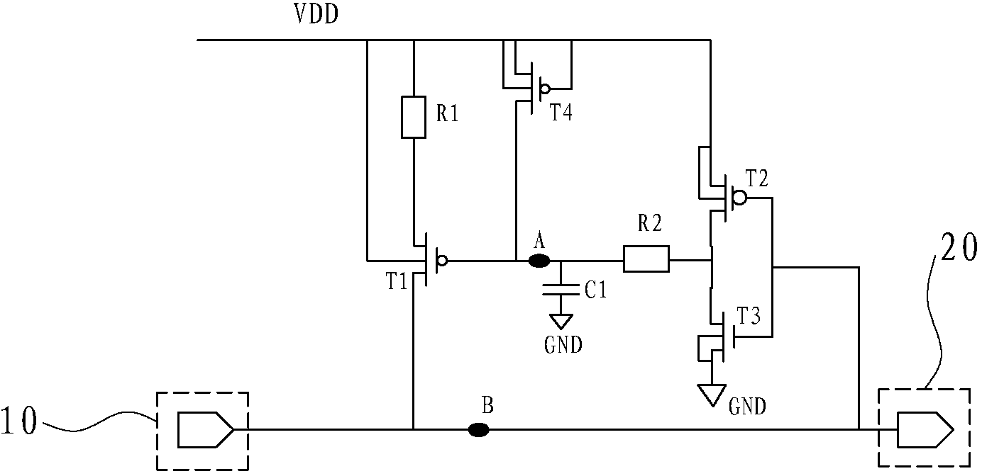
[0025] refer to image 3 As shown, a chip bonding selection circuit without static power consumption disclosed by the present invention includes a PMOS transistor T1, a resistor R1, a capacitor C1, a PMOS transistor T2, an NMOS transistor T3, a resistor R2 and a PMOS transistor T4.

[0026] The D pole of the PMOS transistor T1 is connected to the circuit control terminal 10 and the circuit controlled terminal 20, the circuit control terminal 10 is the chip bonding connection plate, the chip bonding connection plate is suspended or connected to GND; the circuit controlled terminal 20 is the output logic pin , The output logic pin is connected to the chip.

[0027] The S pole of the PMOS transistor T1 is connected in series with the resistor R1 to VDD, the S pole and the G pole of the PMOS transistor T4 and the S pole of the PMOS transistor T2...


PUM


Abstract

The invention discloses a chip routing selection circuit free of quiescent dissipation. The electrode D of a PMOS tube T1 is connected with a circuit control end and a circuit controlled end, and the electrode G of the PMOS tube T1 is connected with a capacitor C1 and one end of a resistor R2, and is further connected with the electrode D of the PMOS tube T1. The electrode S of the PMOS tube T1 is connected with a resistor R1 in series and is connected with a VDD, the electrode S and the electrode G of a PMOS tube T4 and the electrode S of a PMOS tube T2. The other end of the capacitor C1 is connected with the GND. The other end of the resistor R2 is simultaneously connected with the PMOS tube T2 and the electrode D of an NMOS tube T3, the electrode S of the NMOS tube T3 is connected with the GND, and the PMOS tube T2 is connected with the electrode G of the NMOS tube T3 and is connected with the circuit controlled end. One connecting wire is needed only when the circuit control end is connected with the GND, and the quiescent dissipation does not exist whether the circuit control end is connected with the GND or suspended.

Description

technical field [0001] The invention relates to a wire bonding selection circuit, in particular to a chip wire bonding selection circuit without static power consumption. Background technique [0002] In the design of integrated circuits, the internal logic of the chip is often changed by connecting the PAD (bonding area) to GND (power ground), not connecting the wire, or connecting it to VCC (supply voltage), so as to realize a bare chip package into two One or more products with different functions. [0003] Such as figure 1 As shown, the chip bonding selection circuit without static power consumption in the prior art is composed of a resistor R and a Schmitt trigger; one end of the Schmitt trigger is connected to one end of the resistor R, and the other end outputs a logic signal to the chip; The other end is connected to the chip bonding pad (Bonding PAD); the chip bonding pad is connected to VCC through the connecting wire, and the Schmitt trigger outputs a high-level...

Claims


Application Information

Patent Timeline
Patent Type & Authority Applications(China)
IPC IPC(8): H03K19/0185
Inventor 赵东世
Owner SI EN TECH XIAMEN
Why Eureka
Try Eureka