Power-up Overshoot Suppression Circuit Applied to Linear Stabilized Voltage Source

A technology of linear voltage regulator and suppression circuit, which is applied in the field of overshoot circuit, can solve the problems of limited suppression ability and achieve the effect of convenient application, no static power consumption, and no influence of input and output voltage drop

CN103312137BActive Publication Date: 2015-09-23EAST CHINA INST OF OPTOELECTRONICS INTEGRATEDDEVICE
3 Cites 0 Cited by

Patent Information

Authority / Receiving Office
CN · China
Patent Type
Patents(China)
Current Assignee / Owner
Publication Date
2015-09-23

Smart Images

  • Figure 1
    Figure 1
  • Figure 2
    Figure 2
  • Figure 3
    Figure 3
Patent Text Reader

Abstract

The invention relates to a power-on overshoot suppression circuit applied to a linear regulator. The power-on overshoot suppression circuit comprises a power-on delay control module, an inverse ratio pull-down module and a positive feedback module, wherein the power-on delay control module comprises a switching tube, a second field-effect tube, a first resistor, a second resistor and an external regulation capacitor, the source electrode of the switching tube is connected with a power supply system, the drain electrode of the switching tube is connected with the source electrode of the second field-effect tube, the grid electrode of the second field-effect tube is grounded after passing through the second resistor and the external regulation capacitor which are connected in series, the first resistor is connected between the source electrode and the grid electrode of the second field-effect tube in parallel, the inverse ratio pull-down module is connected between the drain electrode of the second field-effect tube and the ground, the positive feedback module is connected between the drain electrode of the second field-effect tube and the grid electrode of the switching tube, and the drain electrode of the switching tube is connected with the input end of the linear regulator. The power-on overshoot suppression circuit has the advantages of enabling the linear regulator to work after a power supply becomes stable and effectively suppressing power-on overshoot, being convenient for being interfaced with a linear regulator circuit and being convenient to apply.
Need to check novelty before this filing date? Find Prior Art

Description

technical field

[0001] The invention relates to a circuit for eliminating overshoot when a linear voltage stabilizer is powered on. Background technique

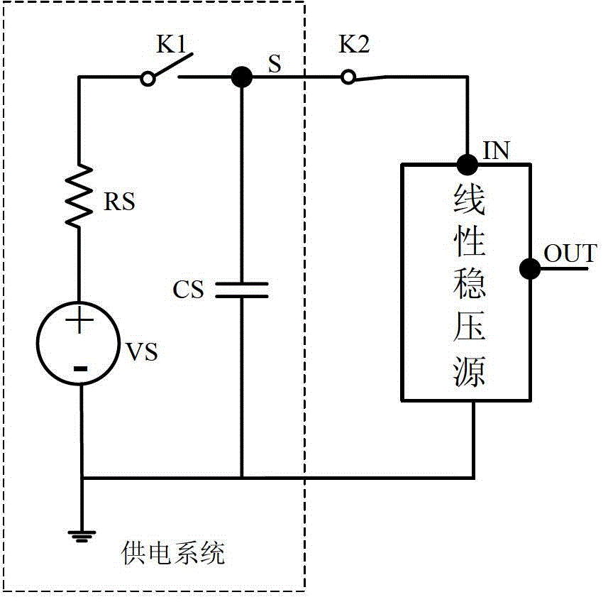
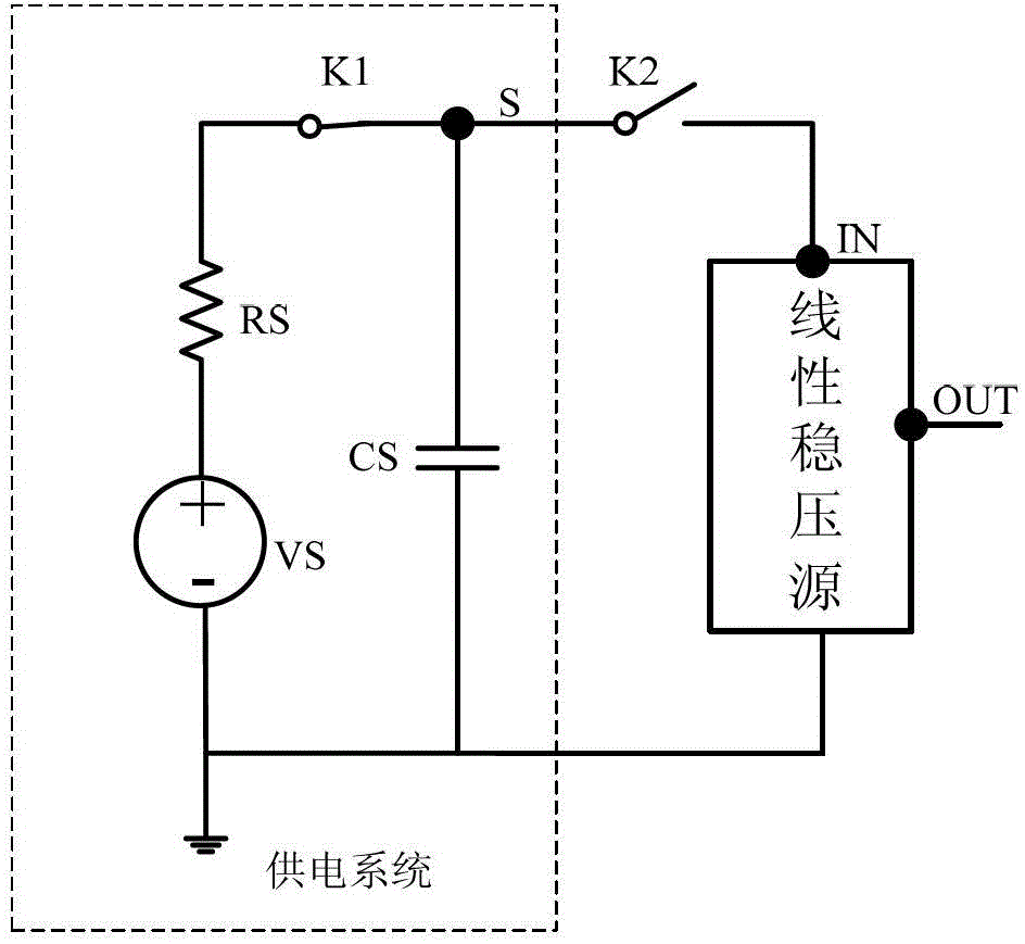
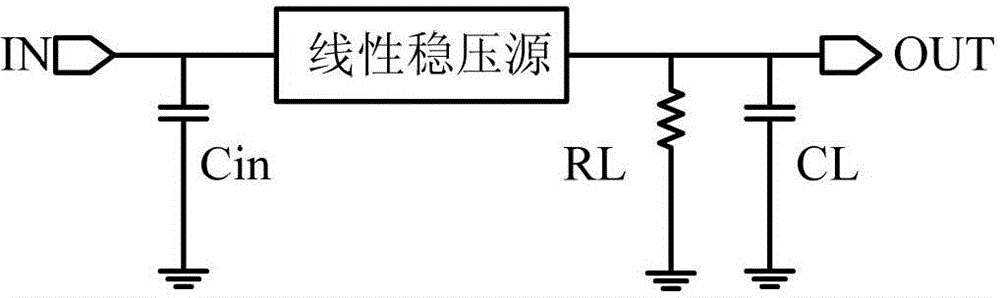
[0002] See attached figure 1 And attached figure 2 As shown, the dotted line is the equivalent circuit diagram of a typical power supply system. for figure 1 , the switch K1 is closed, and the power supply system supplies power to the linear regulated source. Since the capacitor Cs is usually large, the voltage at point S will not change abruptly, and the linear regulated source has a good power-on output. when using figure 2 When supplying power to the outside world, the typical application diagram of its linear voltage regulator is as follows: image 3 As shown, the external power supply current at point S and the voltage at the IN terminal will change suddenly, and the gate (base) voltage of the drive tube of some linear voltage regulators will change abnormally, resulting in power-on overshoot of the linear volt...

Examples

Embodiment 1

[0022] Embodiment one: see attached Figure 5 And attached Image 6 shown. A power-on overshoot suppression circuit applied to a linear voltage stabilizer is arranged between a power supply system and an input end of the linear voltage stabilizer.

[0023] The power-on overshoot suppression circuit applied to a linear voltage regulator includes a power-on delay control module, an inverse ratio pull-down module and a positive feedback module.

[0024] The power-on delay control module includes a switch tube P1, a second field effect transistor P2, a first resistor R1, a second resistor R2, and an external adjustment capacitor C. The source of the switching transistor P1 is connected to the power supply system, and the drain of the switching transistor P1 is connected to the source of the second field effect transistor P2. The gate of the second field effect transistor P2 is grounded after being connected in series with the second resistor R2 and the external adjustment capac...