Chip carrier for semiconductor chip

a technology of semiconductor chips and carriers, applied in semiconductor devices, semiconductor/solid-state device details, electrical devices, etc., can solve the problems of reducing the package yield and other serious problems, and achieve the effect of preventing the formation of voids

Active Publication Date: 2006-09-05
SILICONWARE PRECISION IND CO LTD
View PDF4 Cites 99 Cited by
  • Summary
  • Abstract
  • Description
  • Claims
  • Application Information

AI Technical Summary

Benefits of technology

[0006]A primary objective of the present invention is to provide a chip carrier for a semiconductor chip, with a plurality of solder mask openings having different sizes being formed on the chip carrier to correspond to differently sized pitches between solder pads, so as to reduce formation of voids during an underfill process.
[0007]Another objective of the present invention is to provide a chip carrier for a semiconductor chip, with a plurality of solder mask openings having different sizes being formed on the chip carrier to correspond to differently sized pitches between solder pads, so as to prevent an bridging effect between bumps caused by voids formed in the pitches and assure the quality of products.
[0009]Compared to the prior art, the chip carrier in the present invention is formed with solder mask openings having different sizes to correspond to differently sized pitches between the adjacent solder pads on the chip carrier, so as to prevent formation of voids during an underfill process.

Problems solved by technology

Although the above-mentioned technique can solve the problem of reducing the pitch between the adjacent solder pads, other serious problems are incurred as a result of variously sized pitches between the solder pads.
Subsequently, as shown in FIG. 1f, an undesirable bridging effect between the metal bumps may be caused by the voids 15 between the adjacent metal bumps 16 during subsequent reflow and surface-mount technology (SMT) processes, thereby reducing the package yield.
Therefore, the problem to be solved here is to provide a chip carrier with bumps pads being arranged in differently sized pitches so as to prevent formation of voids due to differently sized pitches between the solder pads during an underfill process.

Method used


Image

  • Chip carrier for semiconductor chip
  • Chip carrier for semiconductor chip
  • Chip carrier for semiconductor chip

Examples


Embodiment Construction

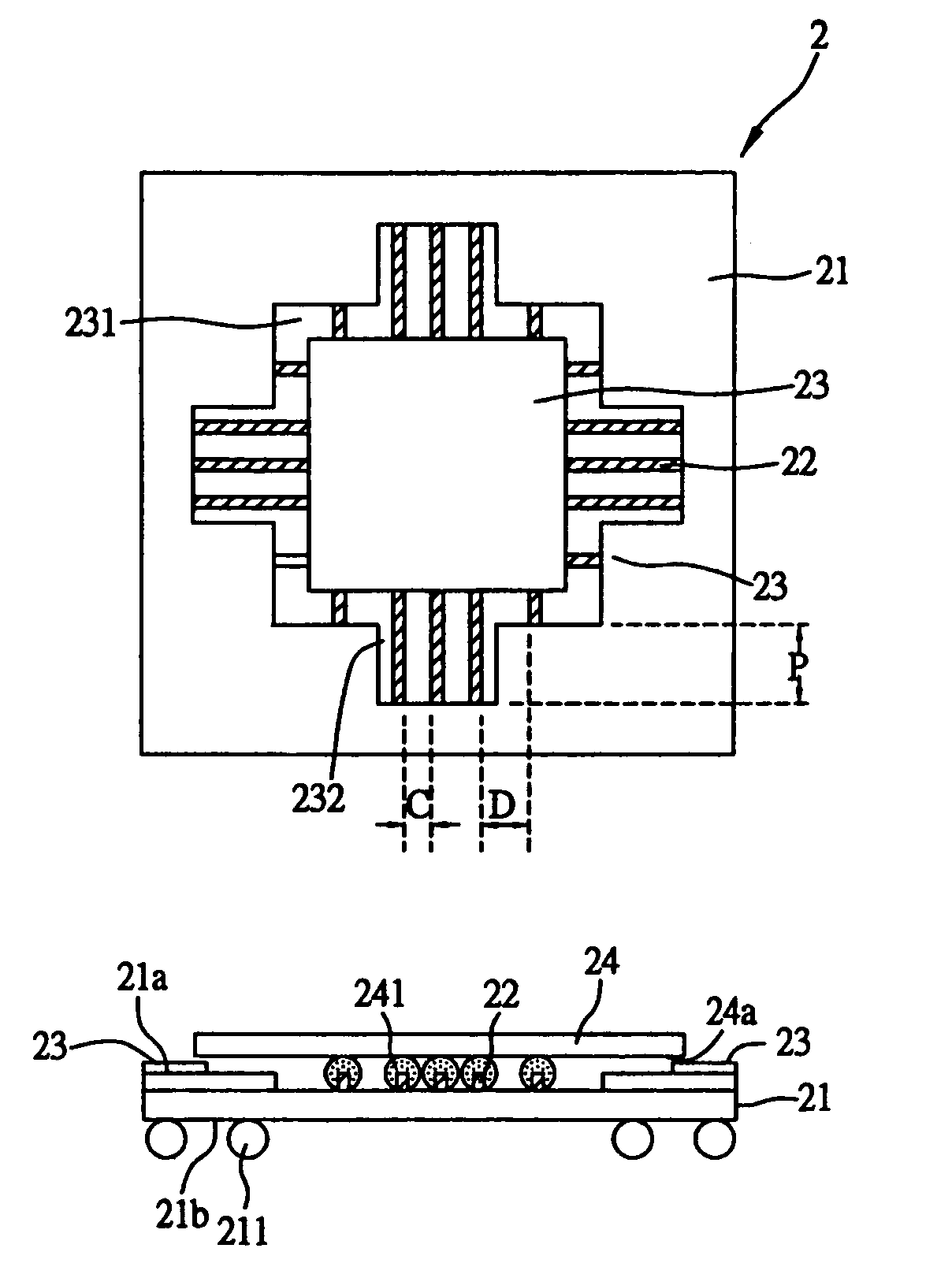
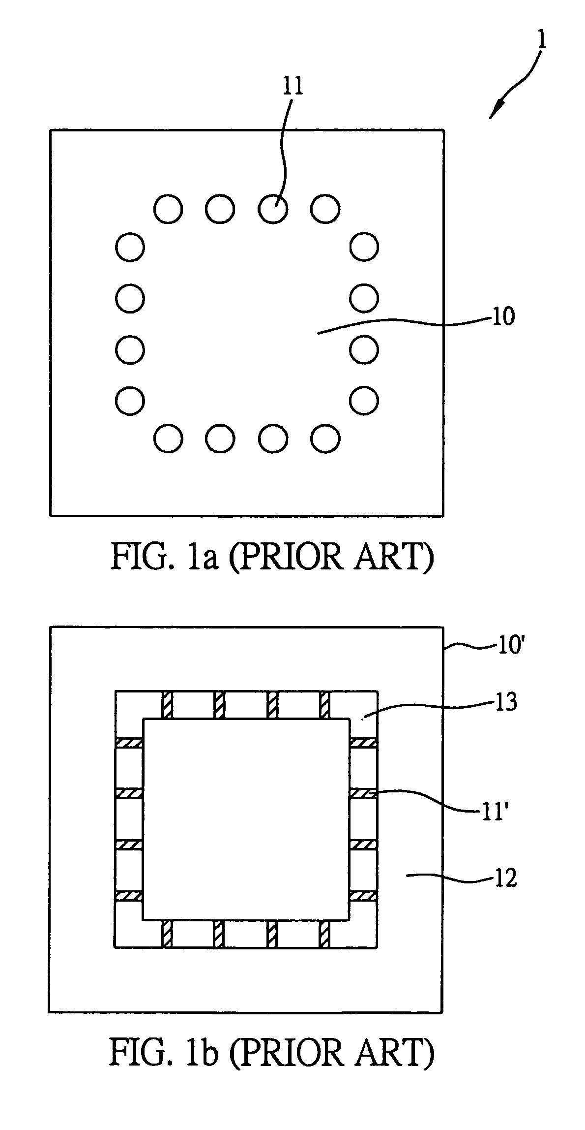
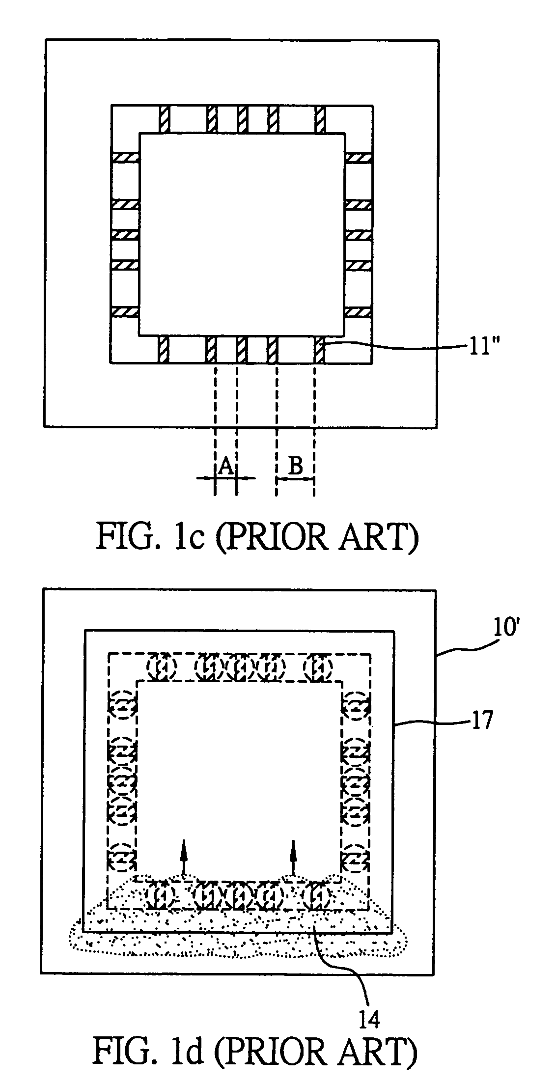
[0016]FIGS. 2 and 3 show a chip carrier 2 for a semiconductor chip according to a preferred embodiment of the present invention. It is to be noted here that the above drawings and other drawings depicted in the specification are made in simplicity and only showing the components related to the chip carrier in the present invention. The actual layout and fabrication processes for the semiconductor package should be more complicated and are not to be further described herein.

[0017]In this embodiment, as shown in FIGS. 2 and 3, the chip carrier 2 comprises a chip carrier body 21, a plurality of solder pads 22, and a solder mask layer 23.

[0018]The chip carrier body 21 serves as a medium for establishing an electrical connection between the semiconductor package and an external device. In this embodiment, the chip carrier body 21 may be a ball grid array (BGA) substrate. The chip carrier body 21 has a first surface 21a electrically connected to electronic elements, and a second surface 2...


PUM


Abstract

A chip carrier for a semiconductor chip is provided. A plurality of solder pads for bump soldering are formed on a chip mounting surface of the chip carrier, to allow a flip chip to be mounted and electrically connected to the chip carrier. A solder mask layer is formed on the chip carrier, wherein a plurality of openings are provided in the solder mask layer to expose the solder pads, and an outwardly opening extended portion is formed respectively from the openings corresponding to the solder pads having a relatively narrower pitch therebetween, so as to prevent formation of voids during an underfill process for filing a gap between the flip chip and the chip carrier.

Description

FIELD OF THE INVENTION[0001]The present invention relates to chip carriers for semiconductor chips, and more particularly, to a chip carrier for accommodating a semiconductor chip, with solder pads being arranged in differently sized pitches on the chip carrier.BACKGROUND OF THE INVENTION[0002]The current trend for developing electronic products is heading towards fabricating a device with a minimized and compact size, improved functions, and increased input / output connections. Typically, a conventional semiconductor package is fabricated by packaging a single integrated circuit (IC) or semiconductor chip with a lead frame or substrate via processes such as die attach, wire bonding, molding, and trim and form processes, making the size of the fabricated package be several times of that of the semiconductor chip. A later developed flip-chip technology involves forming gold (Au), tin / lead (Sn / Pb) or other metal bumps on the semiconductor chip, allowing the metal bumps to be soldered t...

Claims


Application Information

Patent Timeline
Patent Type & Authority Patents(United States)
IPC IPC(8): H01L23/48H01L23/498
CPCH01L23/49816H01L23/49838H01L2924/15311H01L2924/01079H01L2224/16
Inventor PU, HAN-PINGLIN, CHANG-FUHUANG, CHIEN-PING
Owner SILICONWARE PRECISION IND CO LTD
Why Eureka
Try Eureka