Supercharge Your Innovation With Domain-Expert AI Agents!

Testing device

A technology for testing devices and contact elements, which is applied in the direction of measuring devices, measuring electricity, and measuring electrical variables, etc. It can solve the problems of high testing cost and expensive X-ray equipment, and achieve the effect of low testing cost and accurate test results

Inactive Publication Date: 2013-12-25
HONG FU JIN PRECISION IND (SHENZHEN) CO LTD +1
View PDF0 Cites 3 Cited by
  • Summary
  • Abstract
  • Description
  • Claims
  • Application Information

AI Technical Summary

Problems solved by technology

However, X-ray equipment is expensive, making the test costly

Method used


Image

  • Testing device
  • Testing device
  • Testing device

Examples


Embodiment Construction

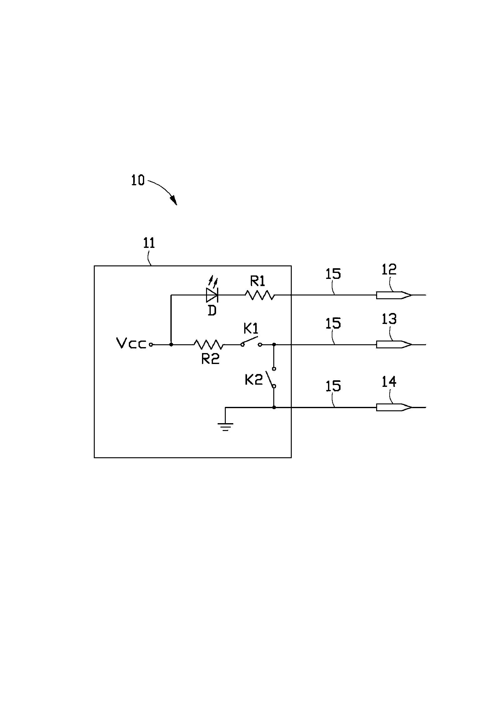
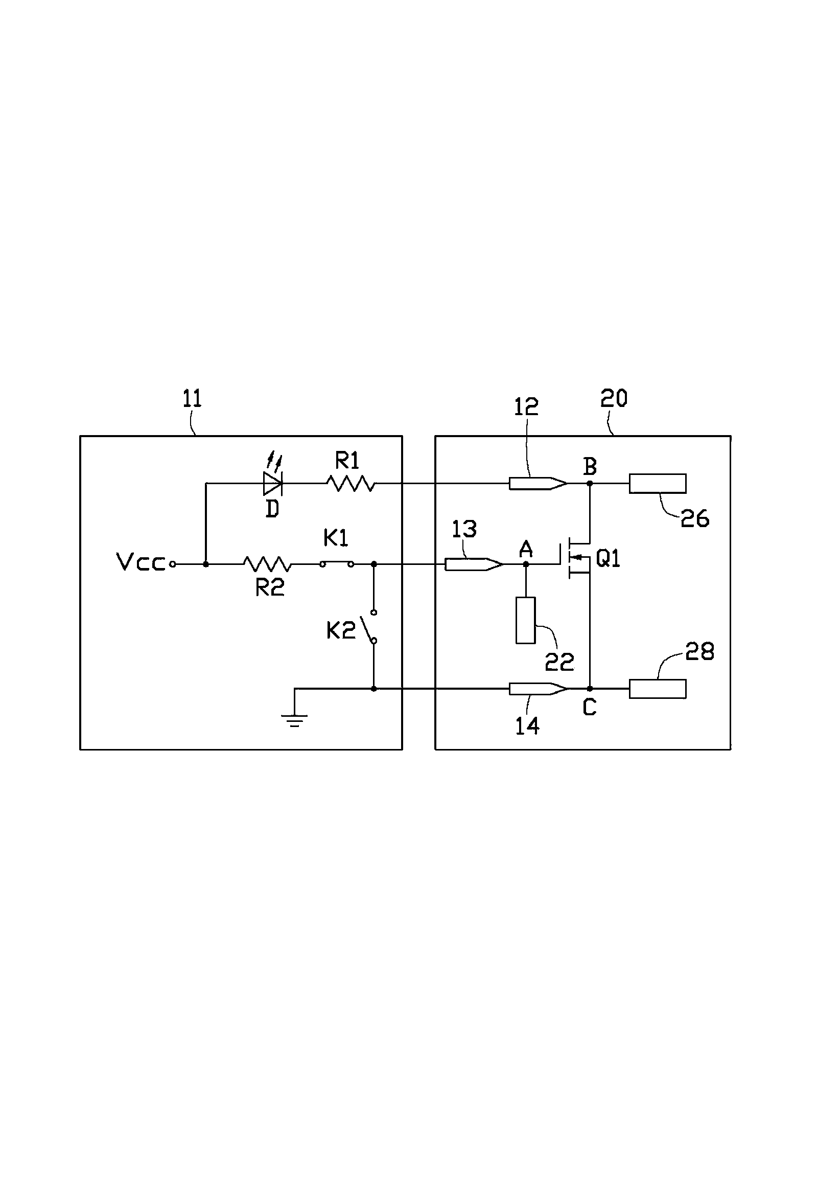
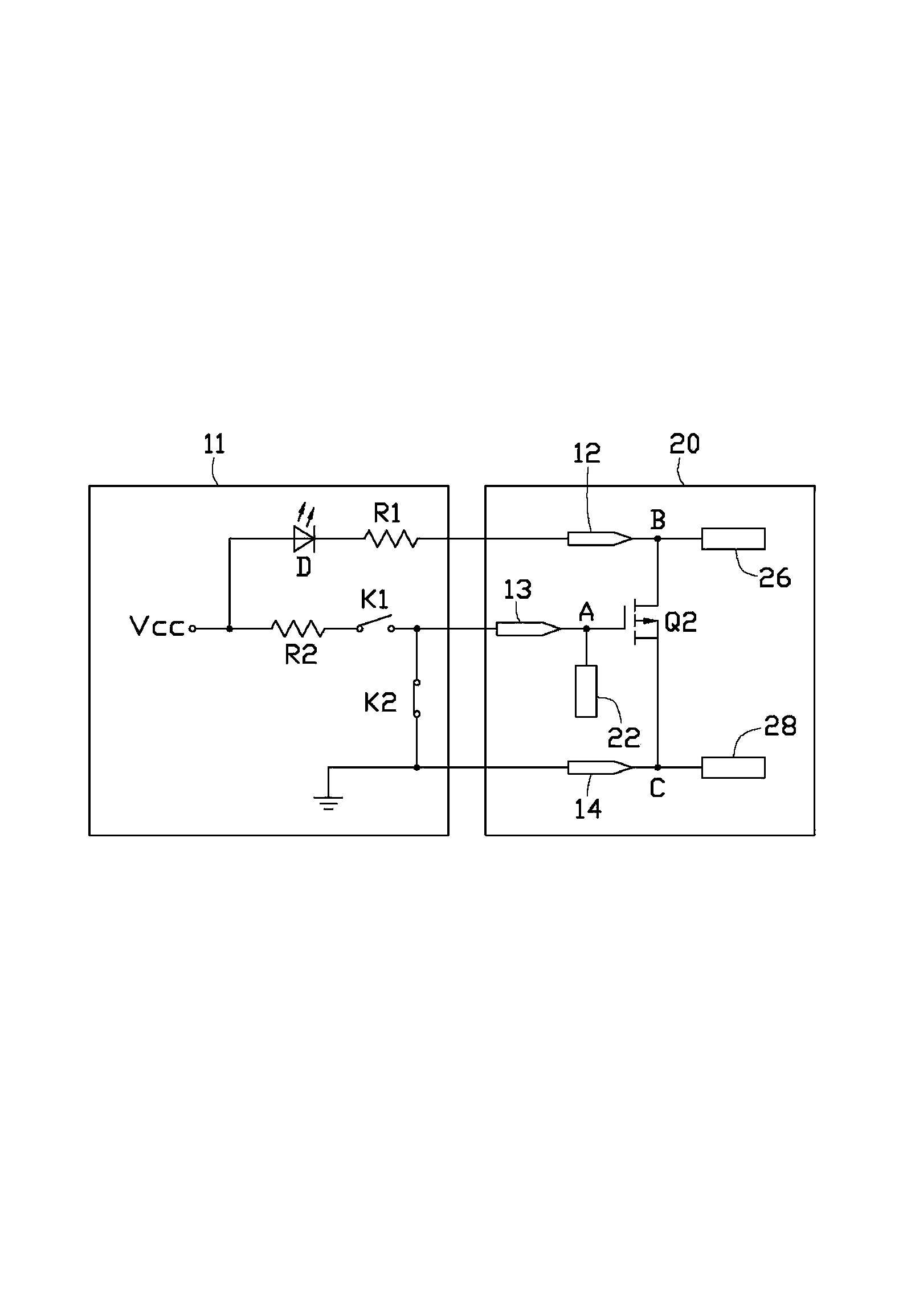
[0013] Please refer to Figure 1 to Figure 3 , the test device 10 of the present invention is used to test whether the MOS transistors packaged by DirectEFT on a circuit board 20 have false soldering or false soldering. A preferred embodiment of the testing device 10 includes a circuit board 11 , a light emitting diode D, two switches K1 , K2 , two resistors R1 , R2 and three contact elements 12 - 14 . The LEDs D, switches K1, K2 and resistors R1, R2 are all set on the circuit board 11, and the contact elements 12-14 are connected to the elements on the circuit board 11 through three cables 15.

[0014] The anode of the LED D is connected to a power supply Vcc. The cathode of the LED D is connected to the contact element 12 through the resistor R1 and the cable 15 . One end of the switch K1 is connected to the power supply Vcc through the resistor R2. The other end of the switch K1 is connected to the contact element 13 through the cable 15 . One end of the switch K2 is co...


PUM


Abstract

A testing device is used to test whether false welding and fake welding exist in a MOS pipe which is welded on a circuit board. The testing device comprises a light emitting diode, a first switch, a second switch, a first resistor, a second resistor, a first contact component, a second contact component and a third contact component. During testing, the first contact component is contacted with a drain electrode of the MOS pipe. The second contact component is contacted with a grid electrode of the MOS pipe. The third contact component is contacted with a source electrode of the MOS pipe. When the MOS pipe is a NMOS pipe, the first switch is closed. When the MOS pipe is a PMOS pipe, the second switch is closed. If the light emitting diode is non-luminance, the false welding and the fake welding exist in the MOS pipe. If the light emitting diode is luminescence, the false welding and the fake welding do not exist in the MOS pipe. By using the testing device, a test result is accurate and test cost is low.

Description

technical field [0001] The invention relates to a test device, in particular to a test device for testing whether a DirectEFT packaged MOS tube is falsely welded or not. Background technique [0002] The MOS tube in the DirectEFT package is widely used because of its advantages of small impedance and fast heat dissipation. However, since the pins of the gate, drain and source of the MOS tube in the DirectEFT package are small and are all located on the bottom of the MOS tube, when the MOS tube in the DirectEFT package is soldered to the circuit board, false soldering and false soldering are prone to occur. . At present, the industry uses X-ray equipment to detect whether the MOS transistors in the DirectEFT package soldered to the circuit board have false soldering or false soldering. However, X-ray equipment is expensive, making testing expensive. Contents of the invention [0003] In view of the above, it is necessary to provide a low-cost test device that can accurat...

Claims


Application Information

Patent Timeline
IPC IPC(8): G01R31/00
Inventor 周海清
Owner HONG FU JIN PRECISION IND (SHENZHEN) CO LTD
Features
  • R&D
  • Intellectual Property
  • Life Sciences
  • Materials
  • Tech Scout
  • Unparalleled Data Quality
  • Higher Quality Content
  • 60% Fewer Hallucinations
Learn More