A kind of additive preparation method of double-sided panel

A double-sided, additive technology, applied in the direction of multi-layer circuit manufacturing, etc., can solve the problems of inability to achieve the conductivity of bulk materials, low conductivity of conductive lines, affecting conductivity, etc., so as to reduce purchase pressure, simplify equipment, reduce The effect of the process flow

Inactive Publication Date: 2016-06-08
FUDAN UNIV
View PDF5 Cites 0 Cited by
  • Summary
  • Abstract
  • Description
  • Claims
  • Application Information

AI Technical Summary

Problems solved by technology

However, there are many problems in this process: the printed conductive ink needs to be sintered at a higher temperature, so that the choice of the substrate is limited to materials with good heat resistance, which cannot be applied to polyester with poor heat resistance, but the cost On the lower substrate; in order to keep the nanoparticles stable in the solution, the conductive ink contains a small amount of organic additives, which makes a lot of impurities remain on the conductive circuit after sintering, which affects the conductive performance
Moreover, there are still many voids and cracks on the conductive circuit after sintering. These factors make the conductivity of the conductive circuit low, far from reaching the conductivity of the bulk material; due to the extremely high specific surface of the nanoparticles, the conductive ink is very easy to be Oxidation, so the nano-copper conductive ink needs a special device to isolate the air during the preparation and sintering process, which greatly increases the production cost; the manufacturing method of inkjet printing is only suitable for the preparation of single-sided printed circuit boards, and is more suitable for use It is very weak in the manufacture of a wide range of double-sided and multi-sided printed circuit boards

Method used


Image

  • A kind of additive preparation method of double-sided panel
  • A kind of additive preparation method of double-sided panel
  • A kind of additive preparation method of double-sided panel

Examples


Embodiment 1

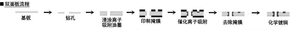
[0034] (1) Use glass fiber cloth epoxy laminate as the substrate, drill holes in the design part, remove flash and burrs, wash with clean water, and dry.

[0035] (2) The substrate after drilling is placed in a container containing 100g / LH 2 SO 4 ,120g / LKMnO 4 Roughen in the coarsening solution at 50 degrees for 30 minutes, take it out, wash it with clean water, and dry it.

[0036] (3) The roughened substrate is immersed in the ion-absorbing ink. The ion-absorbing ink contains 0.1 polyacrylic acid, 0.1 polyvinyl alcohol, and 0.8 water. It is taken out after 30 seconds and placed in an oven for 30 minutes at 70 degrees.

[0037] (4) Use screen printing to print a mask pattern on the substrate after dipping the ion-adsorbing ink to expose the circuit and through hole.

[0038] (5) Place the substrate after printing the mask at 50 degrees 0.05mol / LNa 2 PdCl 4In the aqueous solution for 30 seconds, take it out, wash it with clean water, and dry it.

[0039] (6) The substra...

Embodiment 2

[0045] (1) Select a polyimide flexible substrate, drill holes in the design part, remove flash and burrs, wash with clean water, and dry.

[0046] (2) The substrate after drilling is placed in a 4 Roughen in the coarsening solution at 50 degrees for 30 minutes, take it out, wash it with clean water, and dry it.

[0047] (3) The roughened substrate is immersed in the ion-absorbing ink. The ion-absorbing ink contains 0.05 polyacrylamide, 0.1 polyvinyl butyral, 0.35 water, and 0.5 ethanol. Take it out after 30 seconds, and place it in an oven for 30 minutes at 70 degrees.

[0048] (4) Use laser printing to print a mask pattern on the substrate after dipping the ion-adsorbing ink to expose the circuit and through hole.

[0049] (5) Place the substrate after printing the mask at 50 degrees 0.05mol / LAgNO 3 In the aqueous solution for 30 seconds, take it out, wash it with clean water, and dry it.

[0050] (6) The substrate adsorbing catalytic ions is placed in ethyl acetate to di...

Embodiment 3

[0056] (1) Choose a polyethylene terephthalate flexible substrate, drill holes in the design part, remove flash and burrs, wash with clean water, and dry.

[0057] (2) The substrate after drilling is placed in a roughening solution containing 120g / L NaOH, 60g / L 1,2-propylene glycol to roughen at 50 degrees for 30 minutes, take it out, wash it with clean water, and dry it.

[0058] (3) The roughened substrate is immersed in the ion-absorbing ink. The ion absorbing ink contains 0.05 polyaminosiloxane, 0.05 polybutyl acrylate, 0.05 polyvinyl chloride, 0.25 ethanol, 0.25 butyl acetate, and 0.35 xylene. Take it out after 30 seconds, and put it in the oven for 30 minutes at 70 degrees.

[0059] (4) Use inkjet printing to print a mask pattern on the substrate after dipping the ion-adsorbing ink to expose the circuit and through hole.

[0060] (5) Place the substrate after printing the mask at 50 degrees 0.05mol / LNa 2 PdCl 4 In the aqueous solution for 30 seconds, take it out, was...


PUM


Abstract

The invention belongs to the field of printed electronics. Specifically, it is an additive preparation method for double-sided panels. The steps can be summarized as follows: Drill holes on the required parts of the substrate, apply ion-absorbing ink on the surface of the substrate and inside the holes by dip coating after drilling; print a mask on the substrate by printing after drying , under the cover of the mask, immerse in the catalytic ion solution to absorb catalytic ions; use a solvent to dissolve the mask, put it in the chemical plating solution to metallize the lines and through holes, and obtain the required double-sided board. The invention is an additive preparation process of conductive lines, which does not require metal corrosion and greatly reduces environmental pollution; the lines and through holes are prepared in one process, compared with the traditional process, the lines are prepared first, and then the through holes are prepared. The hole method reduces the process flow and reduces the production cost.

Description

technical field [0001] The invention belongs to the field of printed electronics, and specifically relates to an additive preparation method of a double-sided board. Background technique [0002] The printed circuit board (PCB) is the carrier board for the secondary packaging of electronic components and is one of the most important components in the electronics industry. The conductive circuit on the PCB is manufactured using the photolithographic etching method. The specific process is: heat-press copper foil on one or both sides of the substrate to make a copper-clad laminate; coat the photoresist on the copper-clad laminate, Selective exposure is carried out under the cover of the film; the unexposed photoresist is washed off to expose the underlying copper; the exposed copper is etched away, and then the remaining photoresist is removed to obtain the desired circuit pattern. However, the photolithographic etching method has many disadvantages such as high material cons...

Claims


Application Information

Patent Timeline
Patent Type & Authority Patents(China)
IPC IPC(8): H05K3/46
Inventor 杨振国常煜
Owner FUDAN UNIV
Why Eureka
Try Eureka