
Eureka
For R&D, Eureka makes reading and utilizing patents & technical documents easy.
Eureka AIR
Designed for self-driven R&D workflows. Generate viable solutions, solve complex R&D challenges, empower your innovation with AI.

Eureka Materials
Designed for material experts only. Revolutionize your material R&D, from search, analyze, to developing new materials.

TechResearch
Generate reliable direction feasibility study reports for your R&D in just a few steps.

TechSeek
Discover and master advanced knowledge NOW. Basics, ideas, possibilities, all at once.

TechMind
As an expert in R&D Theories, TechMind can generates customized viable solutions instantly.

TechRisk
Analyze your overall solution with one click, know your potential R&D risks in advance.

TechMonitor
Get weekly tech updates, stay abreast of the latest tech innovations and key insights.
Photoelectric component detection method and detection equipment implementing same
A detection method and technology of detection equipment, which are applied in the parts of electrical measuring instruments, measuring electricity, measuring devices, etc., to achieve accurate measurement values and improve efficiency.
- Summary
- Abstract
- Description
- Claims
- Application Information
AI Technical Summary
Problems solved by technology
Method used
Image

Examples
Embodiment Construction
[0037] The technical contents and features of the present invention will be described in detail below through the enumerated embodiments in conjunction with the accompanying drawings, wherein:
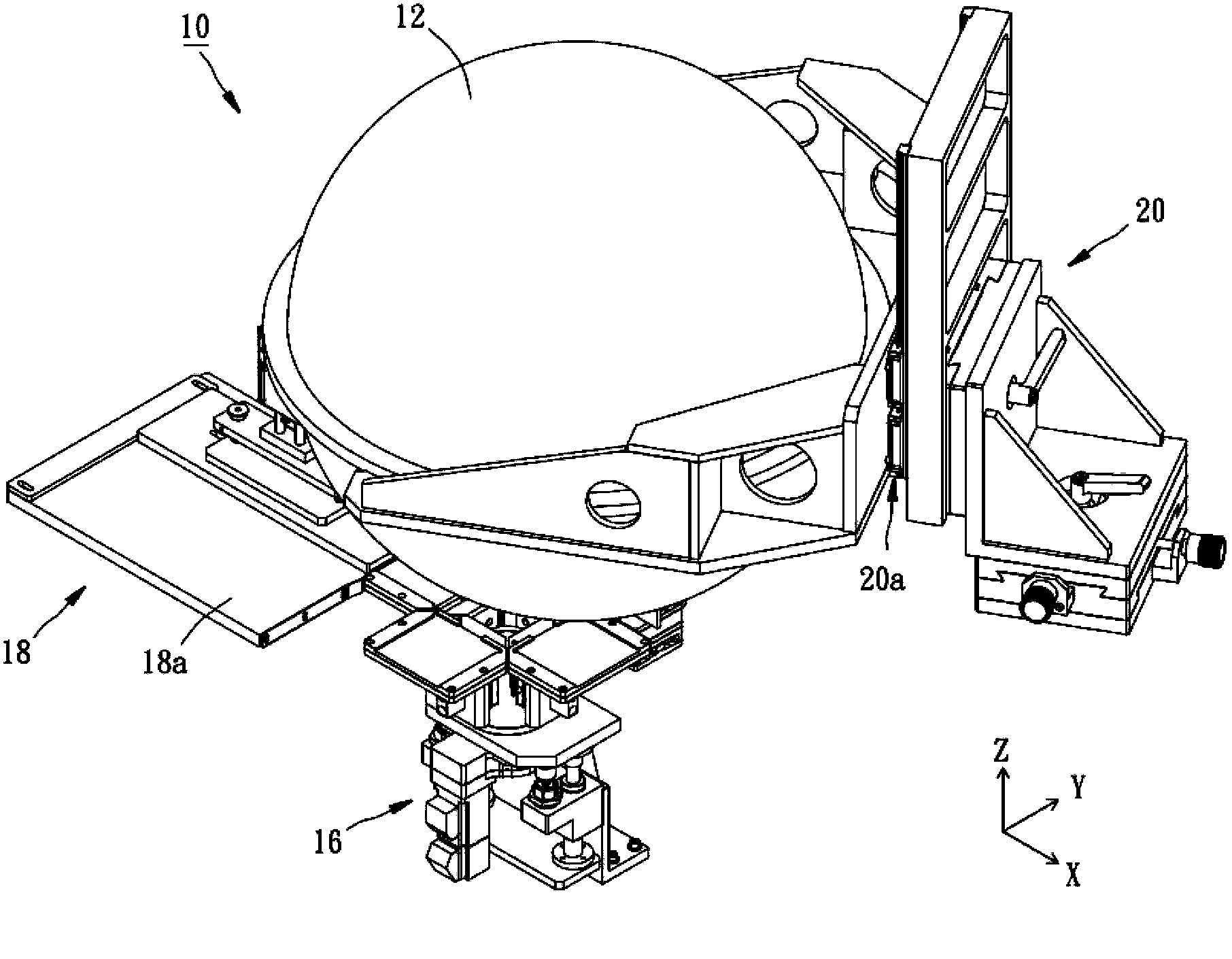
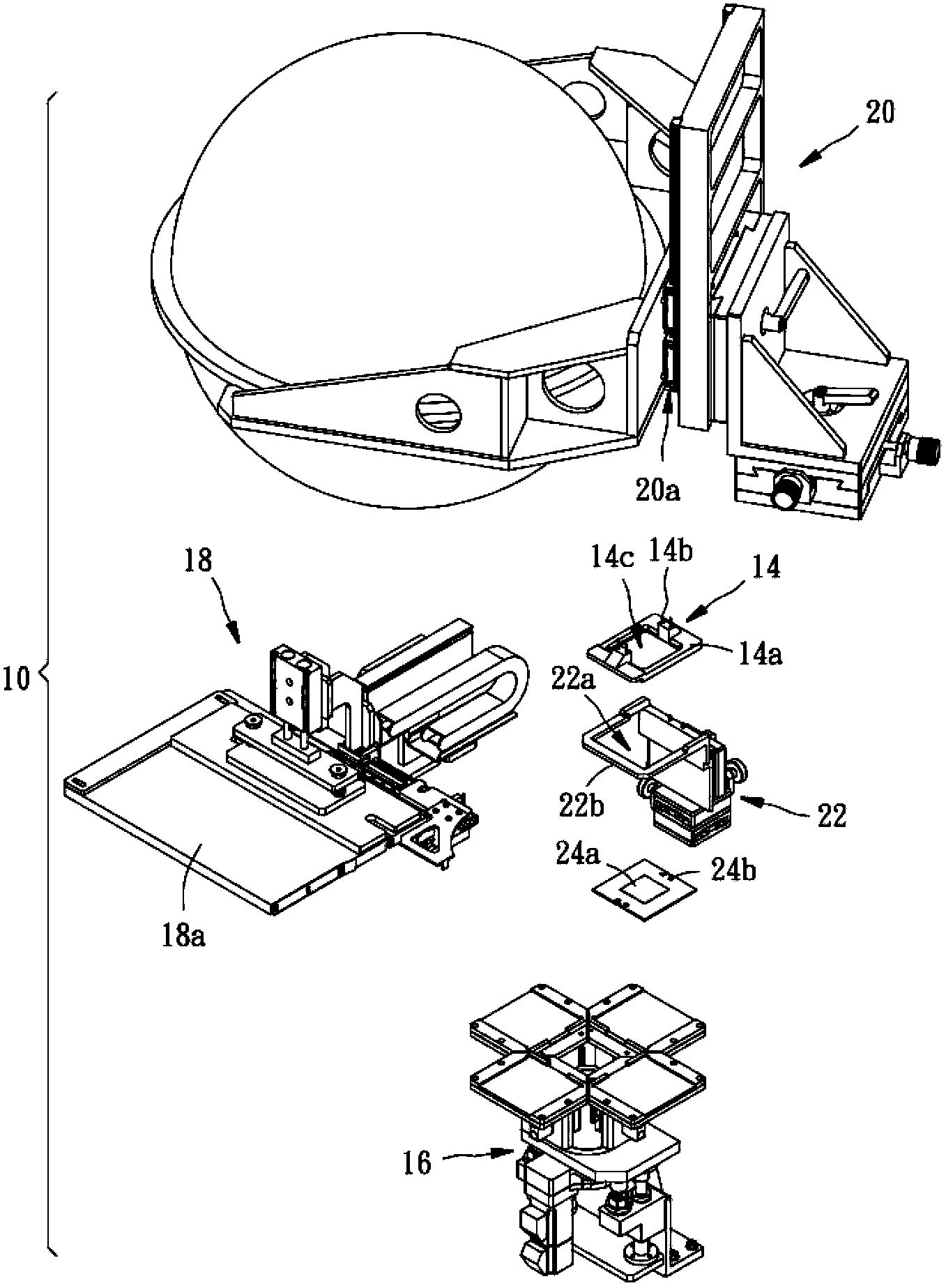
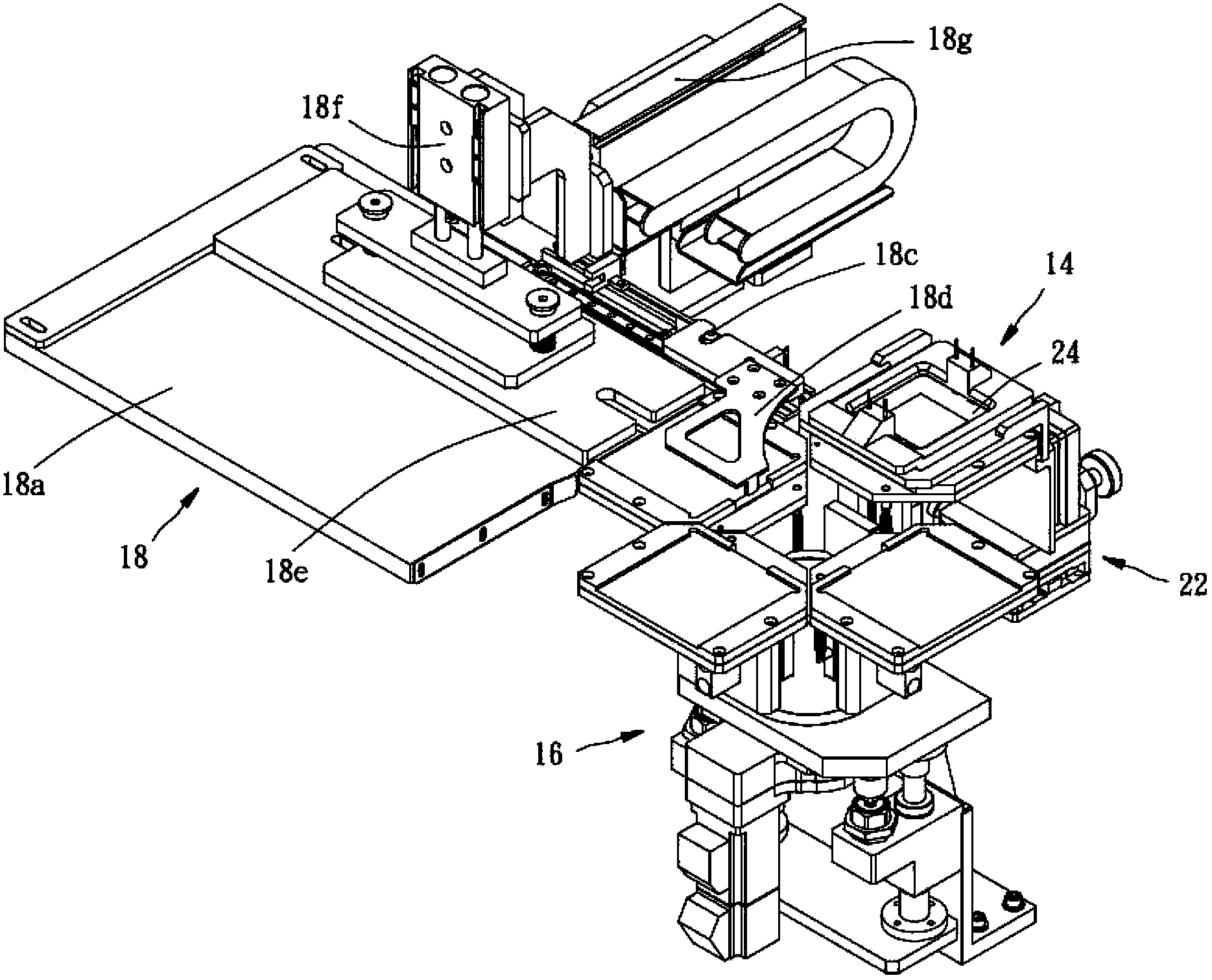
[0038] Figure 1 to Figure 12 , is a schematic diagram illustrating the corresponding relationship between each material carrier plate of the rotary indexing mechanism and each step of the detection method.
[0039] First of all, it must be noted that the optoelectronic components suitable for the detection method provided by the present invention can be (but not limited to) light emitting diode (light emitting diode, LED) package components or package modules, such as chip-on-board ( Chip on Board (COB) packaged LED modules. Secondly, throughout the specification, including the embodiments described below and claims for patent claims, when it is mentioned that one component is "connected" to another component, it means that the component is "directly" fixed to another c...
PUM
 Abstract
Description
Claims
Application Information
 - R&D Engineer
- R&D Manager
- IP Professional
- Industry Leading Data Capabilities
- Powerful AI technology
- Patent DNA Extraction
Browse by: Latest US Patents, China's latest patents, Technical Efficacy Thesaurus, Application Domain, Technology Topic, Popular Technical Reports.
© 2024 PatSnap. All rights reserved.Legal|Privacy policy|Modern Slavery Act Transparency Statement|Sitemap|About US| Contact US: help@patsnap.com