Defect detecting system and method

A technology of defect detection and process equipment, applied in semiconductor/solid-state device testing/measurement, electrical components, semiconductor/solid-state device manufacturing, etc., can solve problems such as waste of defect detection resources and reduced operating efficiency of defect detection equipment 120, and achieve self- Effects of adjusting defect detection, improving operational efficiency, and efficient defect detection

Active Publication Date: 2014-01-01
SHANGHAI HUALI MICROELECTRONICS CORP
View PDF6 Cites 6 Cited by
  • Summary
  • Abstract
  • Description
  • Claims
  • Application Information

AI Technical Summary

Problems solved by technology

However, in view of many factors, such as fault maintenance, technical verification, etc., some process equipment may be operated under the condition that certain leases or certain process units are stopped
Therefore, when the process equipment 110 that can operate at most 4 groups of cavities at the same time has only two groups of cavities, if the

Method used


Image

  • Defect detecting system and method
  • Defect detecting system and method
  • Defect detecting system and method

Examples


Embodiment Construction

[0022] In order to make the purpose, technical solution and advantages of the present invention clearer, the following will further describe the implementation of the present invention in detail in conjunction with the accompanying drawings.

[0023] Those skilled in the art can easily understand other advantages and effects of the present invention from the contents disclosed in this specification. The present invention can also be implemented or applied through other different specific implementation modes, and various modifications or changes can be made to the details in this specification based on different viewpoints and applications without departing from the spirit of the present invention.

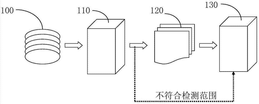
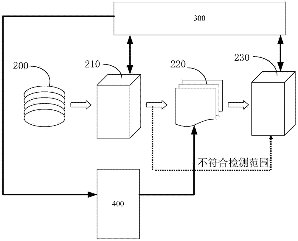
[0024] Figure 2a It is a schematic diagram of the first embodiment of the defect detection system provided by the present invention.

[0025] Such as Figure 2a As shown, the defect detection system provided in this specific embodiment includes: process equipment 210, which is ...


PUM


Abstract

The invention relates to the technical field of semiconductors, and discloses a defect detecting system and method. According to the method, a process device operation information database connected with a production management system is established, information of operation cavities of all process devices is collected and stored in the database, meanwhile, the database is further connected with all the defect detecting devices, the number of wafers for defect detection is defined according to the number of operation cavities of process devices of wafer products, and the number of the wafers is transmitted to the defect detection devices. Compared with the prior art, when a certain or a set of cavities of the process devices can not normally work due to various reasons of the process devices, the process device operation information database defines the number of wafer products for defect detection according to the number of actual operation cavities of the process devices, spot check rules of the defect detecting devices are timely regulated, defect detection operation efficiency is effectively improved, detection resources are saved, and dynamic and self-adjustable effective defect detection is achieved.

Description

technical field [0001] The invention relates to the field of semiconductor technology, in particular to a defect detection system and method in semiconductor technology. Background technique [0002] With the development of integrated circuit technology and the continuous reduction of feature size, the integration of semiconductor chips continues to increase. Integrated circuit design has developed from transistor integration to logic gate integration, and further developed to IP integration. The integration of chips is getting higher and higher. , the distribution of circuits on the chip is becoming more and more complex. Under this development trend, defects in the chip manufacturing process have an increasing impact on chip functions, and some defects can even lead to complete destruction of the entire chip. At the same time, slight changes in equipment performance during the production process will cause resulting in the scrapping of the entire wafer. Therefore, in ord...

Claims


Application Information

Patent Timeline
IPC IPC(8): H01L21/67H01L21/66
CPCH01L21/67253H01L22/12H01L22/20
Inventor 倪棋梁陈宏璘龙吟
Owner SHANGHAI HUALI MICROELECTRONICS CORP
Why Eureka
Try Eureka