Method for making non-conducting hole in inner layer of multilayer PCB board

A technology of PCB board and manufacturing method, which is applied in the direction of printed circuit manufacturing, electrical components, printed circuit, etc., can solve the problems of insufficient support force at the position of large NP holes, unqualified PCB boards, and easy formation of hole halos, etc., to achieve internal support The effect of strengthening force, improving reliability, and improving lamination quality

Active Publication Date: 2016-08-17
GUANGDONG SHENGYI SCI TECH
View PDF4 Cites 0 Cited by
  • Summary
  • Abstract
  • Description
  • Claims
  • Application Information

AI Technical Summary

Problems solved by technology

[0009] The thick copper plate of the multi-layer PCB board opens NP holes (English: None plating hole; Chinese: non-conducting hole), especially the opening of large NP holes is a very serious technical problem with hole halos. The inner layer (that is, the first substrate layer inside the PCB board) has no copper pad, and the internal support force of the large NP hole after lamination is not enough, so that the resistance to the impact of the drill is relatively weak when drilling, so it is easy to form a hole halo At the same time, due to the thick copper of each inner layer (the position of the NP hole is a copper-free area), under the action of the buffer material during lamination, since the position of the NP hole is in the copper-free layer area, the NP position (the position of the copper-free area) The thickness is thinner than other positions (where there is a copper layer area) (for large NP holes, it is about 20-40um thinner), so when drilling holes, a certain gap is formed between the plate and the backing plate on the table of the mechanical drilling machine, which is difficult for processing NP The hole, especially the large NP hole, is very unfavorable, and it is easy to form a hole halo; thus, the processed NP hole is unqualified, and the entire PCB board is unqualified

Method used


Image

  • Method for making non-conducting hole in inner layer of multilayer PCB board
  • Method for making non-conducting hole in inner layer of multilayer PCB board

Examples


Embodiment Construction

[0020] Embodiments of the present invention will now be described with reference to the drawings, in which like reference numerals represent like elements.

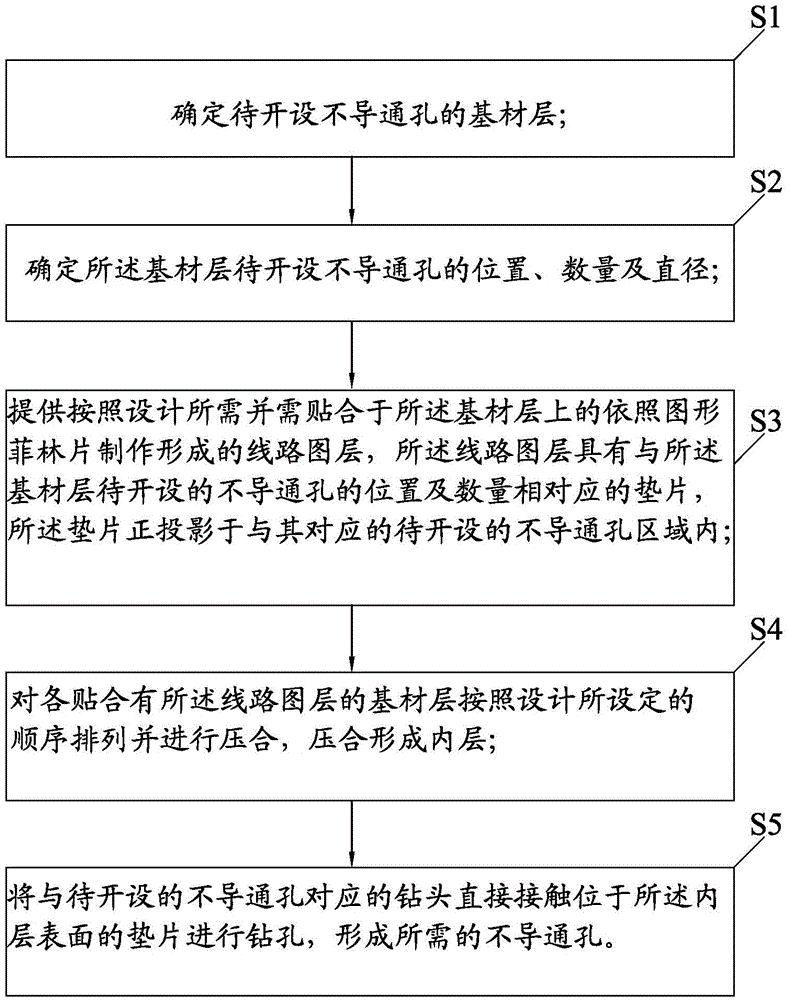
[0021] Such as figure 1 As shown, the method for making the non-conducting hole in the inner layer of the multilayer PCB of the present invention comprises the following steps:

[0022] (S1) Determine the substrate layer to be opened with non-conducting holes;

[0023] (S2) determining the position, quantity and diameter of the non-conducting holes to be opened in the substrate layer;

[0024] (S3) Provide a circuit layer formed according to the graphic film sheet that needs to be attached to the substrate layer according to the design, and the circuit layer has a non-conductive hole to be opened with the substrate layer The pads corresponding to the position and quantity of the pads, the pads are orthographically projected in the area of ​​the corresponding non-conducting hole to be opened; (S4) for each substrate laye...


PUM


Abstract

The invention discloses a method for making a non-conductive hole in the inner layer of a multilayer PCB, which comprises the following steps: (1) determining the substrate layer to be opened with a non-conductive hole; (2) determining the substrate layer to be opened with a non-conductive hole; The position, quantity and diameter of the through holes; (3) Provide a circuit layer formed according to the graphic film sheet that is required by the design and needs to be attached to the substrate layer. The circuit layer has non-conducting holes to be opened Gaskets corresponding to the position and quantity of the gaskets, the gaskets are orthographically projected in the area of ​​the non-conducting hole; (4) Each substrate layer bonded with the circuit layer is pressed to form an inner layer; ( 5) Directly contact the gasket on the surface of the inner layer for drilling to form the required non-conductive hole; because there is a gasket at the position of the non-conductive hole to be opened before drilling, the internal support force and resistance to drilling The impact of the knife is strengthened, which avoids the hole halo when drilling, and the spacer disappears after the non-conductive hole is drilled, while not changing the original design of the PCB.

Description

technical field [0001] The invention relates to a method for manufacturing a hole in a PCB board, in particular to a method for manufacturing a non-conducting hole in an inner layer of a multilayer PCB board. Background technique [0002] Printed circuit board (English: Printed circuit board; abbreviation: PCB board), PCB board is divided according to the number of layers, which can be divided into three categories: single-sided PCB board, double-sided PCB board and multi-layer PCB board. [0003] The single-sided PCB board is the most basic PCB board, and its parts are concentrated on one side of the insulating base material layer as the base material, and the circuit layer is concentrated on the other side of the base material layer. Because the circuit layer (generally formed by etching copper clad laminate, see later) only appears on one side, so this kind of PCB board is a single-sided PCB board. Single-sided PCB boards are usually simple to manufacture and low in cost...

Claims


Application Information

Patent Timeline
Patent Type & Authority Patents(China)
IPC IPC(8): H05K3/00
Inventor 温东华杨波
Owner GUANGDONG SHENGYI SCI TECH
Why Eureka
Try Eureka