Manufacturing method of multi-layer PCB (printed circuit board)

A manufacturing method and multi-layer board technology, applied in the direction of multi-layer circuit manufacturing, etc., can solve the problem of PCB multi-layer board not working normally.

Active Publication Date: 2014-01-22
东莞康源电子有限公司
View PDF4 Cites 5 Cited by
  • Summary
  • Abstract
  • Description
  • Claims
  • Application Information

AI Technical Summary

Problems solved by technology

It can meet the requirements for ordinary products, but for products with a small unit (about 2mm), it can no longer meet the requirements, and it is easy to cause the PCB multilayer board to not work normally.

Method used


Image

  • Manufacturing method of multi-layer PCB (printed circuit board)

Examples


Embodiment Construction

[0009] In order to make the object, technical solution and advantages of the present invention clearer, the present invention will be further described in detail below in conjunction with the accompanying drawings and embodiments. It should be understood that the specific embodiments described here are only used to explain the present invention, not to limit the present invention.

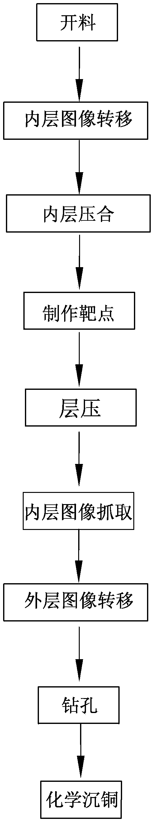
[0010] Such as figure 1 Shown, it is the PCB multilayer board manufacturing method of the present invention, is used for the making of PCB multilayer board, and preserves the alignment accuracy between boards, and it comprises the following steps to complete the making of PCB multilayer board:

[0011] Step 1: Cut the material, choose the appropriate panel and cutting method, and maximize the utilization rate of the panel. The panel includes the inner substrate and the inner copper foil attached to the upper and lower surfaces of the inner substrate.

[0012] Step 2: Inner layer image transfer, ap...


PUM


Abstract

A manufacturing method of a multi-layer PCB comprises the steps as follows: 1), board cutting is performed, so that a jointed board is formed; 2), an inner-layer image is transferred; 3), inner-layer press fit is performed; 4), a target point is manufactured: a part of an exposed inner-layer copper foil of an inner-layer circuit image is manufactured into a special image, so that the target point is manufactured; 5), lamination is performed; 6), the inner-layer image is captured: a CCD (charge coupled device) image sensor is used for capturing the target point on the inner-layer copper coil, and position information of the target point is stored in a computer; 7), an outer-layer image is transferred: the target point on the inner-layer copper foil is captured through the CCD image sensor and taken as a reference, and an outer-layer circuit image is formed; 8), drilling is performed; and 9), chemical copper deposition is performed, and the inner-layer circuit image and the outer-layer circuit image are conducted. The target point is manufactured on a part of the copper foil of the inner-layer circuit image, and when the outer-layer image is transferred, the target point on the inner-layer copper foil is taken as a reference, so that the accuracy of the outer-layer circuit image and the inner-layer circuit image is guaranteed.

Description

technical field [0001] The invention relates to a method for manufacturing a multilayer board, in particular to a method for manufacturing a PCB multilayer board. Background technique [0002] At present, in the industry, when the outer layer image of the PCB multilayer board is produced, the outer layer image transfer is usually positioned by the outer layer hole, and the alignment between the inner layer circuit layer and the outer layer circuit layer is generally between 4-5mil. In the subsequent drilling step, this method has the problem that the hole is offset from the inner layer pattern. It can meet the requirements for ordinary products, but for products with a small unit (about 2mm), it can no longer meet the requirements, and it is easy to cause the PCB multilayer board to fail to work normally. Contents of the invention [0003] Based on this, it is necessary to provide a method for manufacturing a PCB multilayer board to address the deficiencies in the prior a...

Claims


Application Information

Patent Timeline
Patent Type & Authority Applications(China)
IPC IPC(8): H05K3/46
Inventor 陈松杜军杨建勇
Owner 东莞康源电子有限公司
Why Eureka
Try Eureka