A memory device structure and preparation method of electrical programming-ultraviolet light erasing
A storage device and ultraviolet light technology, which is applied in the direction of electrical solid-state devices, semiconductor/solid-state device manufacturing, electrical components, etc., can solve the problem of low device erasing efficiency, improve erasing efficiency and working speed, expand application space, Possibility-enhancing effects
- Summary
- Abstract
- Description
- Claims
- Application Information
AI Technical Summary
Problems solved by technology
Method used
Image
Examples
Embodiment 1
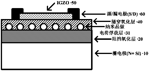
[0068] Step 1: Select a heavily doped N-type single crystal silicon wafer with a resistivity of 0.008~0.100 Ω cm as the substrate, and clean the silicon wafer through a standard RCA cleaning process, and then use hydrofluoric acid to remove the surface of the silicon wafer oxide layer.
[0069] Step 2: On the cleaned silicon wafer, use ALD method to deposit and grow Al 2 o 3 The thin film acts as a blocking oxide layer for the memory. Al 2 o 3 The thickness of the film is 20~150nm; during the deposition process, the substrate temperature is controlled between 100~300 ℃; 2 o 3 The reaction sources are trimethylaluminum and water vapor.
[0070] Step 3: Using ALD method on Al 2 o 3 A layer of Pt nanocrystals is deposited on the film as the charge trapping layer of the memory. The reaction sources for the deposition of Pt nanocrystals are (MeCp)Pt(Me)3 and O 2 , the deposition temperature is 200~400°C, and the number of deposition cycles is 10~100.
[0071] Step 4: Dep...
Embodiment 2
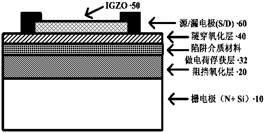
[0081] Step 1: Select a heavily doped N-type single crystal silicon wafer with a resistivity of 0.008~0.100 Ω cm as the substrate, and clean the silicon wafer through a standard RCA cleaning process, and then use hydrofluoric acid to remove the surface of the silicon wafer oxide layer.
[0082] Step 2: On the cleaned silicon wafer, use ALD method to deposit and grow Al 2 o 3 The thin film acts as a blocking oxide layer for the memory. al 2 o 3 The thickness of the film is 20~150nm; during the deposition process, the substrate temperature is controlled between 100~300°C; the growth of Al 2 o 3 The reaction sources are trimethylaluminum and water vapor.
[0083] Step 3: Using ALD method on Al 2 o 3 A layer of ZnAlO film with a thickness of 10-50nm is deposited on the film as the charge trapping layer of the memory. The reaction sources for depositing ZnAlO thin films are trimethylaluminum, diethylzinc and water vapor, and the deposition temperature is 100~300°C. During ...
PUM
 Abstract
Description
Claims
Application Information


