Memory chip, imaging box, serial number replacement method and method for using memory chip

A technology for storing chips and serial numbers, which is applied to equipment of electrical recording technology using charge patterns, electrical recording technology applying charge patterns, electrical recording techniques, etc., can solve problems such as inconvenient operation, increased cost, and small selection of modules , to achieve the effect of improving user experience and solving unusable

Active Publication Date: 2014-03-19
APEX MICROELECTRONICS CO LTD
View PDF7 Cites 54 Cited by
  • Summary
  • Abstract
  • Description
  • Claims
  • Application Information

AI Technical Summary

Problems solved by technology

However, some imaging devices will record dozens of serial numbers. At this time, if you still use jumpers or combination switches to select, the selection module will become extremely large and complicated, which will undoubtedly increase the cost and increase the difficulty of manufacturing.
Even if the memory chip only stores two serial numbers, suc...

Method used


Image

  • Memory chip, imaging box, serial number replacement method and method for using memory chip
  • Memory chip, imaging box, serial number replacement method and method for using memory chip
  • Memory chip, imaging box, serial number replacement method and method for using memory chip

Examples


Embodiment 1

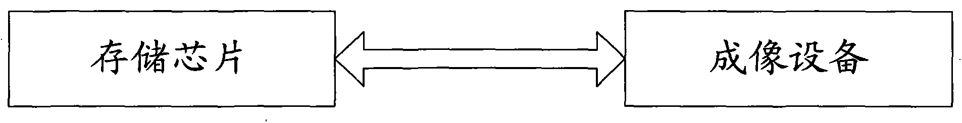
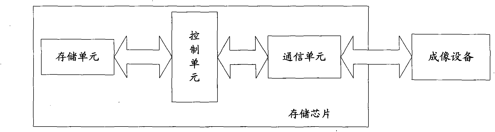
[0051] The present invention provides a storage chip for imaging box, such as figure 2 As shown, the imaging box is detachably installed on the imaging device, and the storage chip includes: a communication unit, a control unit and a storage unit, wherein:

[0052] The communication unit is used for receiving information sent by the imaging device and sending information to the imaging device. The communication between the communication unit and the imaging device can be a wired connection, that is, a contact method, such as two-way communication through a contact on the memory chip and a contact on the imaging device; it can also be a wireless connection. That is, non-contact methods, such as two-way communication between the coil (antenna) on the memory chip and the coil on the imaging device.

[0053] The storage unit is used to store at least tag information and a plurality of different serial number information. The initial value of the tag information indicates that th...

Embodiment 2

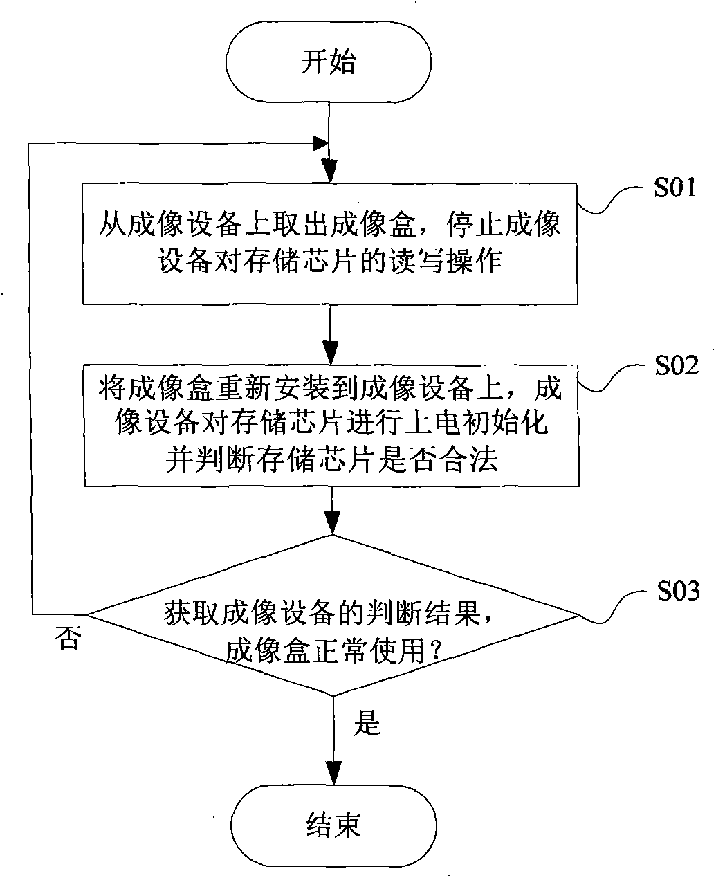
[0081] In the first embodiment, when the storage chip sends the serial number to the imaging device, it is first determined that the serial number is legal (that is, the marking information is not modified), and then the preset strategy is used to determine whether the serial number is really legal. And re-determine whether to continue to select the current serial number as the selected serial number according to the result of judgment. The inventors of the present invention found that modifying some steps can also solve the same problem. That is, when the memory chip sends the serial number to the imaging device, the serial number is first considered to be illegal (that is, the tag information is modified), and then the preset strategy is used to judge whether the serial number is really illegal, and based on the result of the judgment, the serial number is reset. Determine whether to continue selecting the current serial number as the selected serial number. This embodiment...


PUM


Abstract

A memory chip provided by the invention includes a communication unit, a control unit and a storage unit. The invention also provides a method for using the memory chip. A plurality of different pieces of serial number information and marker information/access marker information which indicate whether currently-selected serial number information is valid or not, are stored in a storage unit; a control unit judges whether serial number information that is transmitted to an imaging device is confirmed valid according to a preset strategy; the selected serial number information is independently replaced according to judgment results when preset conditions can be satisfied; and therefore, modes of the replacement of serial numbers of the memory chip can be more convenient, and user experience can be greatly improved, and the problem of incapability of being used of the memory chip caused by the identity of the serial numbers can be solved.

Description

technical field [0001] The invention relates to printing and imaging technology, in particular to a storage chip, an imaging box and a method for using the storage chip. Background technique [0002] With the development of imaging technology, imaging devices like laser printing devices and inkjet printing devices have been widely used. During the imaging process, the imaging device needs the assistance of imaging auxiliary information of the imaging box to complete the imaging process. In addition to being recorded in the imaging device, the imaging auxiliary information of the imaging device is also recorded on the memory chip, such as figure 1 as shown, figure 1 It is a schematic diagram of communication interaction between an imaging device and a storage chip in the prior art. Among them, the memory chip is attached to the imaging box (generally adhered or embedded in the imaging box), the imaging box can be an ink box filled with ink or a toner cartridge filled with ...

Claims


Application Information

Patent Timeline
IPC IPC(8): B41J2/175G03G15/08
CPCB41J2/17546G03G21/1878G03G21/1882G03G21/1892G03G21/1875
Inventor 汪栋杰袁延庆
Owner APEX MICROELECTRONICS CO LTD
Why Eureka
Try Eureka