Microwave plasma chemical vapor deposition device

A technology of chemical vapor deposition and microwave plasma, which is applied in the direction of gaseous chemical plating, metal material coating process, coating, etc., can solve the problem of uneven distribution of gas and meet the needs of large-scale industrial production, high The effect of quality deposited film

Active Publication Date: 2014-03-26
西安德盟特半导体科技有限公司
View PDF3 Cites 13 Cited by
  • Summary
  • Abstract
  • Description
  • Claims
  • Application Information

AI Technical Summary

Problems solved by technology

[0004] The object of the present invention is to provide a microwave plasma chemical vapor deposition device to solve the problem that the gas in the reaction chamber cannot be evenly distributed around the substrate surface

Method used


Image

  • Microwave plasma chemical vapor deposition device
  • Microwave plasma chemical vapor deposition device
  • Microwave plasma chemical vapor deposition device

Examples


Embodiment 1

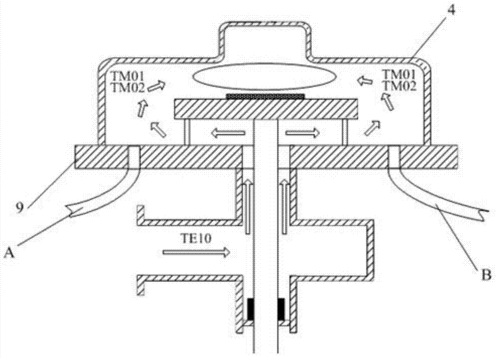
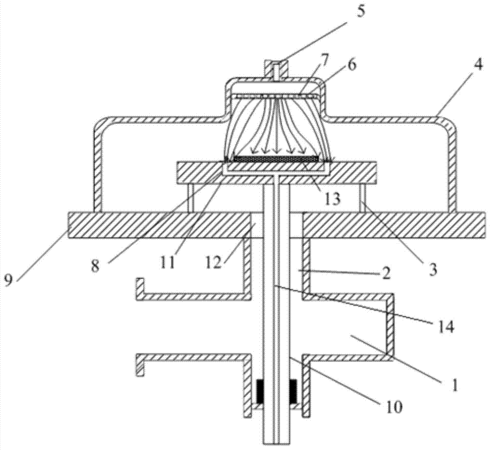
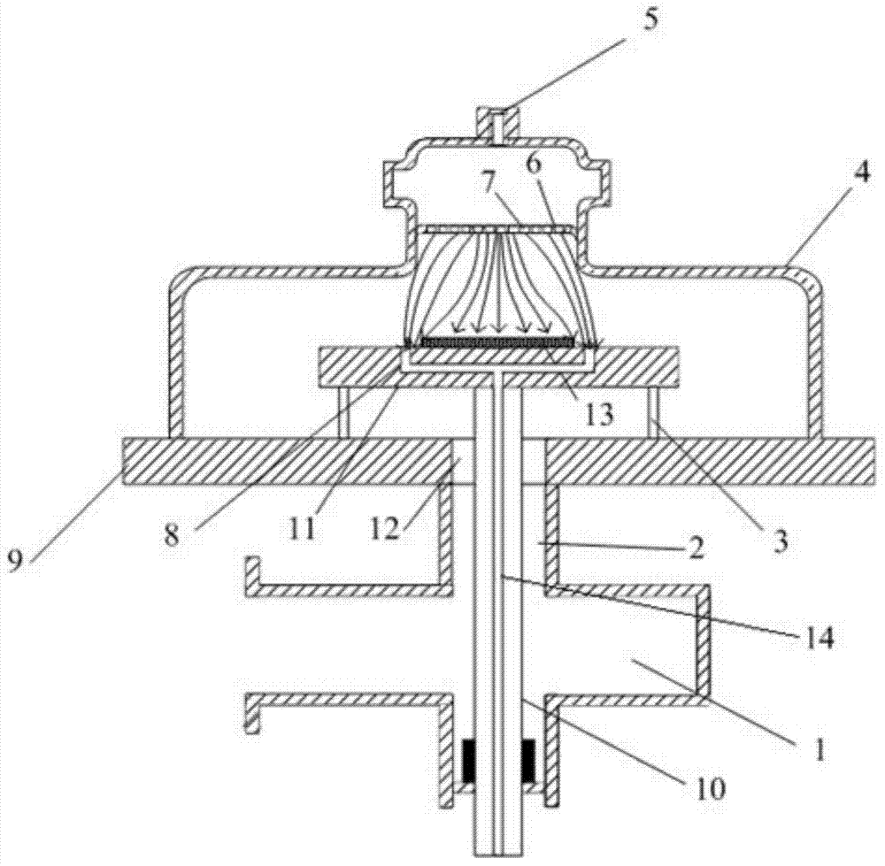
[0025] Such as figure 2 As shown, a microwave plasma chemical vapor deposition device of the present invention includes a reaction chamber composed of a reaction chamber upper cover 4 and a reaction table 9 . A connected rectangular waveguide 1 and coaxial waveguide 2 are arranged below the reaction chamber. The rectangular waveguide 1 is horizontal and used to introduce microwaves from the microwave generator and propagate TE10 single mode. The coaxial waveguide 2 is vertical and uses It is used to couple and propagate TM01 mode and TM02 mode. The reaction table 9 has a through hole 12 with the same shape and size as the inner cavity of the coaxial waveguide 2, the through hole 12 coincides with the exit of the coaxial waveguide 2, and the central axis 10 of the coaxial waveguide 2 extends into the reaction chamber through the through hole 12 .

[0026] A sample stage 11 for placing a substrate 13 is coaxially and fixedly connected above the central axis 10 . An annular q...

Embodiment 2

[0037] Such as Figure 7 As shown, the exhaust channel includes a plurality of vertical exhaust holes 8 that are evenly distributed around the circumference and are located on the sample stage 11 adjacent to the outer edge of the substrate 13. The plurality of vertical exhaust holes 8 are all connected to the The annular gas channel below it is connected, and the annular gas channel is connected with a quartz tube 15 through a horizontal exhaust channel opened radially to the outside. Station 9 is connected to external pipe fittings. combine Figure 8 As shown in , the number of horizontal exhaust passages is four and arranged in the shape of a "ten". Preferably, the diameter of the air inlet hole 7 is 1 mm, and the diameter of the vertical exhaust hole 8 is 1.5 mm.

[0038] A microwave plasma chemical vapor deposition device provided by the present invention improves the effect and efficiency of deposition and film formation, improves the quality and increases the uniformi...


PUM

PropertyMeasurementUnit
diameteraaaaaaaaaa
widthaaaaaaaaaa

Abstract

The invention discloses a microwave plasma chemical vapor deposition device. The device comprises a reaction chamber consisting of a reaction chamber upper cover and a reaction table, wherein a rectangular waveguide and a coaxial waveguide which are connected with each other are arranged below the reaction chamber; a center shaft of the coaxial waveguide extends into the reaction chamber, and a sample table for placing a substrate is coaxially and fixedly connected above the center shaft; a gas guide inlet is formed in the center of the reaction chamber upper cover, a horizontal baffle in which a plurality of small inlet holes are formed is also arranged at the neck of the reaction chamber upper cover, a gas buffering and mixing chamber is formed between the horizontal baffle and the top of the reaction chamber upper cover, and exhaust paths are evenly and circumferentially distributed in positions, which are next to the outer side of the edge of the substrate, of the sample table. According to the device, the problem that gases in the reaction chamber cannot be evenly distributed around the substrate is solved.

Description

technical field [0001] The invention relates to the field of microwave plasma processing, in particular to a microwave plasma chemical vapor deposition device. Background technique [0002] Microwave plasma is a kind of plasma formed by using microwave energy to ionize gas: the gas in the reaction chamber starts to ionize under the excitation of microwave energy, forming a mixture of atoms, atomic groups, ions and electrons. Chemical vapor deposition (Chemical vapor deposition, referred to as CVD) is a process technology in which reacting substances are ionized or decomposed under gaseous conditions, react on the surface of the substrate and form a solid film deposition, and then obtain a solid material. Microwave plasma CVD is a kind of equipment that uses microwave energy to realize chemical vapor deposition. It has the advantages of large output, high quality and low cost. The gas is ionized, forming a plasma, which then forms a solid deposition of species on the substra...

Claims


Application Information

Patent Timeline
Patent Type & Authority Applications(China)
IPC IPC(8): C23C16/455C23C16/511
Inventor 王宏兴
Owner 西安德盟特半导体科技有限公司
Why Eureka
Try Eureka