Forming method of metal gate, forming method of MOS transistor and forming method of CMOS structure

一种金属栅极、金属层的技术,应用在半导体器件、半导体/固态器件制造、电气元件等方向,能够解决高K栅介质层与硅衬底界面缺陷等问题,达到正偏压温度不稳定性降低、负偏压温度不稳定性降低的效果

Active Publication Date: 2014-03-26
SEMICON MFG INT (SHANGHAI) CORP
View PDF8 Cites 33 Cited by
  • Summary
  • Abstract
  • Description
  • Claims
  • Application Information

AI Technical Summary

Problems solved by technology

[0003] However, since the high-K gate dielectric layer is mostly metal ion oxide, and there is no fixed atomic coordination, the bonding between it and the silicon substrate is more stable than that of SiO 2 Compared with the stability of the bonding between the silicon substrate, it is much worse, resulting in a large number of interface defects between the high-K gate dielectric layer and the silicon substrate

Method used


Image

  • Forming method of metal gate, forming method of MOS transistor and forming method of CMOS structure
  • Forming method of metal gate, forming method of MOS transistor and forming method of CMOS structure
  • Forming method of metal gate, forming method of MOS transistor and forming method of CMOS structure

Examples


no. 1 example

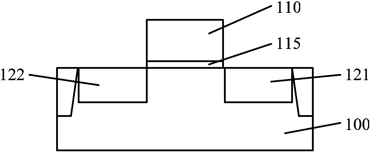
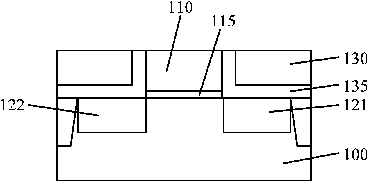
[0027] Please refer to Figure 1 to Figure 8 , is a schematic flowchart of the formation process of the MOS transistor with a metal gate according to the first embodiment of the present invention.

[0028] Please refer to figure 1 , providing a semiconductor substrate 100, forming a second silicon oxide layer 115 on the surface of the semiconductor substrate 100, forming a polysilicon dummy gate 110 on the surface of the second silicon oxide layer 115, and semiconductors on both sides of the polysilicon dummy gate 110 A source 121 and a drain 122 are formed in the substrate 100 .

[0029] The semiconductor substrate 100 is a silicon substrate, a germanium substrate, a silicon nitride substrate or a silicon-on-insulator substrate or the like. Those skilled in the art can select the type of the semiconductor substrate 100 according to the semiconductor devices formed on the semiconductor substrate 100 , so the type of the semiconductor substrate should not limit the protection...

no. 2 example

[0060] Please refer to Figure 9 to Figure 16 , is a schematic flowchart of the formation process of the CMOS structure with a metal gate according to the second embodiment of the present invention.

[0061] Please refer to Figure 9 , provide a semiconductor substrate 200, the semiconductor substrate 200 has a first region 201 and a second region 202, a second silicon oxide layer 215 is formed on the surface of the semiconductor substrate 200, and the first region 201 on the first region 201 A first polysilicon dummy gate 211 is formed on the surface of the silicon dioxide layer 215, a second polysilicon dummy gate 212 is formed on the surface of the second silicon oxide layer 215 on the second region 202, and a second polysilicon dummy gate 212 is formed on the surface of the first polysilicon A first source 221 and a first drain 222 are formed in the semiconductor substrate 200 on both sides of the dummy gate 211, and a second source 223 and a second drain 222 are formed i...


PUM


Abstract

The invention discloses a forming method of a metal gate, a forming method of an MOS (metal oxide semiconductor) transistor and a forming method of a CMOS (complementary metal oxide semiconductor) structure. The forming method of the metal gate comprises the following steps: after removing a pseudo polycrystalline silicon gate and forming a groove, forming high-K gate medium layers at the bottom and on the side wall of the groove, fluoridizing the high-K gate medium layers, and forming a function layer and a metal layer on the surfaces of the high-K gate medium layers. As fluorine bonds such as fluorine-silicon bonds and fluorine-hafnium bonds can be formed among the high-K gate medium layers and a semiconductor substrate after fluoridization and the bond energy of the fluorine bonds is higher than that of original hydrogen bonds, the instability of the negative bias temperature of a device is reduced; as fluorine is strong in oxidability, oxygen vacancies can be prevented from generating donor level in a band gap and becoming positively charged oxygen vacancies, the oxygen vacancies are passivated, and the instability of the positive bias temperature of the device is reduced.

Description

technical field [0001] The invention relates to the field of semiconductor manufacturing, in particular to a method for forming a metal gate, a method for forming a MOS transistor with a corresponding metal gate, and a method for forming a CMOS structure. Background technique [0002] With the continuous development of semiconductor technology, the feature size of MOS transistors is continuously reduced, and the thickness of the gate dielectric layer of MOS transistors is also becoming thinner and thinner according to the principle of proportional reduction. When the thickness of the gate dielectric layer is thin enough to a certain To a certain extent, its reliability issues, especially time-related breakdown, hot carrier effect, diffusion of impurities in the gate electrode to the substrate, etc., will seriously affect the stability and reliability of the device. Now, SiO 2 layer as a gate dielectric layer has reached its physical limit, using a high-K gate dielectric lay...

Claims


Application Information

Patent Timeline
Patent Type & Authority Applications(China)
IPC IPC(8): H01L21/28H01L21/336H01L21/8238
CPCH01L21/28185H01L21/28194H01L21/823842H01L29/517H01L29/66545H01L29/513H01L21/8238H01L29/78
Inventor 李凤莲倪景华
Owner SEMICON MFG INT (SHANGHAI) CORP
Why Eureka
Try Eureka