Automatic skip-stop detection system

A detection system, a technology of jumping goods, applied in the direction of semiconductor/solid-state device testing/measurement, electrical components, circuits, etc., can solve the problems of unable to detect the production line, products cannot be detected, low detection accuracy, etc., to improve the detection accuracy and detection efficiency, improve detection efficiency and detection accuracy

Active Publication Date: 2014-03-26
SHANGHAI HUALI MICROELECTRONICS CORP
View PDF6 Cites 17 Cited by
  • Summary
  • Abstract
  • Description
  • Claims
  • Application Information

AI Technical Summary

Problems solved by technology

But this also leads to a problem: Since the site can pass and test at most 200 batches of products a day, it cannot meet the testing requirements for all 300 batches of products in one day, and the extra 100 batches of products will be directly lost. After testing or the yield engineer artificially skips the station and enters the next process; if there are seriously defective products in the 100 batches of products, because they have not been tested, the yield engineer cannot find the defective products in time and find out the defects that lead to the products The corresponding equipment, and then the products produced by the problematic equipment will also cause defects, thereby reducing the product yield
[0006] At the same time, due to the unevenness of the products on the production line, many lots (batches) produced by different machines at the same site may enter the YE (Yield Enhancement, yield improvement) scanning site at the same time, and the yield engineer artificially checks the redundant 100 batches of products Bounced goods may prevent the products produced by multiple machines from being detected, and the products of some machines are repeatedly sampled, resulting in the narrowing of the detection range; there are also products entering the YE scanning site with different priorities, an

Method used


Image

  • Automatic skip-stop detection system
  • Automatic skip-stop detection system
  • Automatic skip-stop detection system

Examples


Embodiment Construction

[0022] The specific embodiment of the present invention will be further described below in conjunction with accompanying drawing:

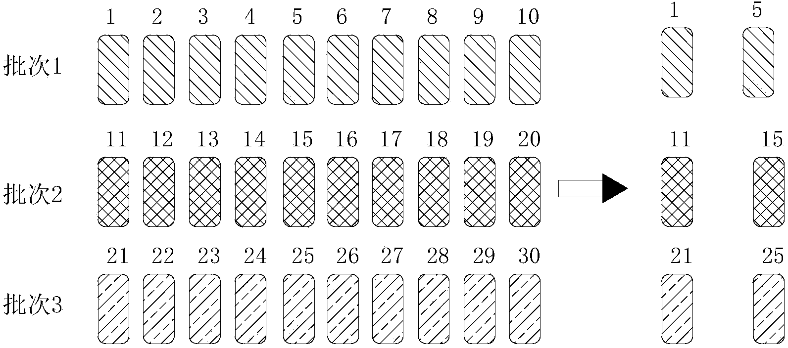
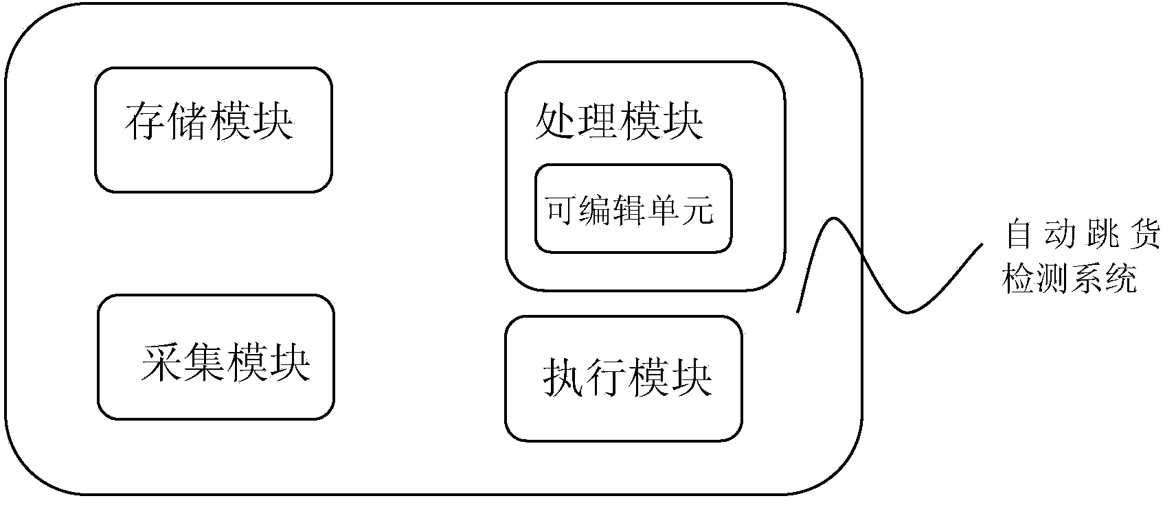
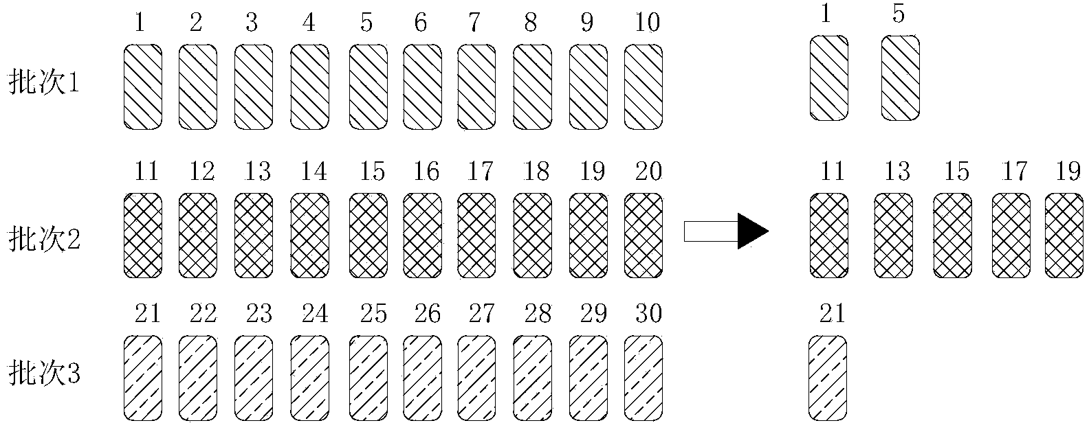
[0023] The invention discloses an automatic skipping detection system, which detects multiple batches of products at any detection station, such as figure 2 As shown, the system includes a storage module, an acquisition module, a processing module and an execution module;

[0024] The storage module stores all production machine information on the production line;

[0025] The acquisition module is used to scan each batch of products passing through the site and obtain the machine information corresponding to the batch of products through the storage module; specifically, the acquisition module scans some products of each batch of products flowing through the site, and Compare with the information of each machine stored in the storage module to obtain the machine from which the batch of products came from;

[0026] The processing module selects...


PUM


Abstract

The invention provides an automatic skip-stop detection system capable of detecting multiple lots of products on any detection station. The automatic skip-stop detection system is characterized by comprising a storage module, an acquisition module, a processing module and an execution module; information of various stations is stored by the storage module; the acquisition module is used for scanning each lot of products passing through the station and acquiring corresponding station information of the products through the storage module; the processing module is used for selecting different sampling detection rules according to the station corresponding to the lot of products; the execution module is used for detecting the products. Different sampling detection rules are set to realize sampling detection of different lots of products according to lot difference and importance degree of the corresponding production stations, so that detection precision and detection efficiency are improved.

Description

technical field [0001] The invention relates to the field of semiconductor detection, in particular to an automatic skipping detection system, which can automatically screen the number of products entering the station of important machine products, and better monitor the production line to make it run more efficiently. Background technique [0002] Semiconductor production is a very complicated process. The main job of the yield engineer is to monitor the normal operation of the production line and to quickly and timely discover various abnormalities on the production line. The yield engineer has to scan a large number of products on the production line to find out Various problems on the production line. [0003] The industry now generally adopts different measurement stations. Each defect scanning station corresponds to a machine or a product of the same machine, and each station sets a ratio. One of the machine products enters (arrives) the inspection During the site, th...

Claims


Application Information

Patent Timeline
IPC IPC(8): H01L21/66
CPCH01L22/30
Inventor 何理许向辉郭贤权陈超
Owner SHANGHAI HUALI MICROELECTRONICS CORP
Why Eureka
Try Eureka