LED packaged piece and manufacturing method thereof

A technology for an LED package and a manufacturing method, which is applied to electrical components, electric solid-state devices, semiconductor devices, etc., can solve the problems of fragile glass tubes, difficulty and risks in the assembly process, and avoid inaccurate alignment and reduce borders. Width, the effect of reducing the difficulty of assembly

Active Publication Date: 2014-03-26
TCL CHINA STAR OPTOELECTRONICS TECH CO LTD
View PDF2 Cites 27 Cited by
  • Summary
  • Abstract
  • Description
  • Claims
  • Application Information

AI Technical Summary

Problems solved by technology

Due to the fragile nature of the glass tube of the quantum strip 302, there are great difficulties and risks in the assembly process

Method used


Image

  • LED packaged piece and manufacturing method thereof
  • LED packaged piece and manufacturing method thereof
  • LED packaged piece and manufacturing method thereof

Examples


Embodiment Construction

[0041] In order to further illustrate the technical means adopted by the present invention and its effects, the following describes in detail in conjunction with preferred embodiments of the present invention and accompanying drawings.

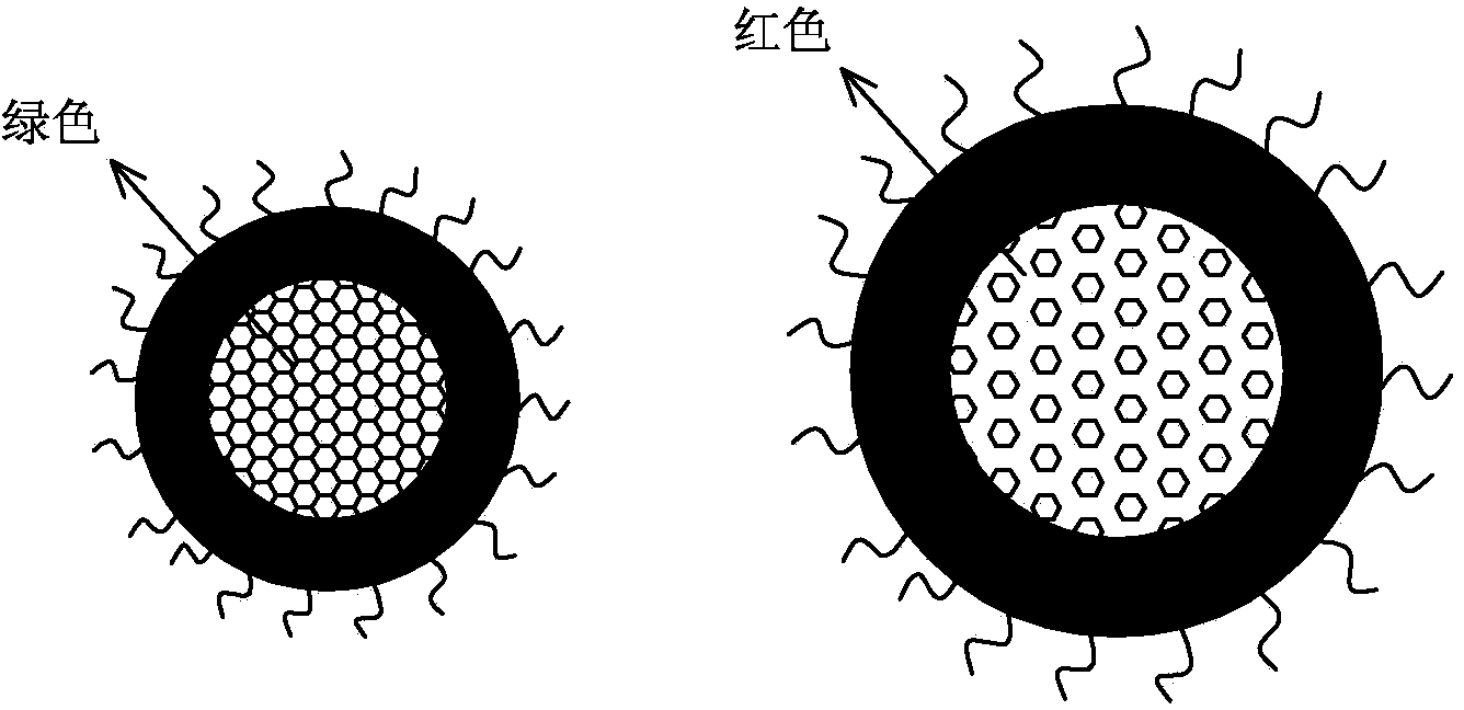
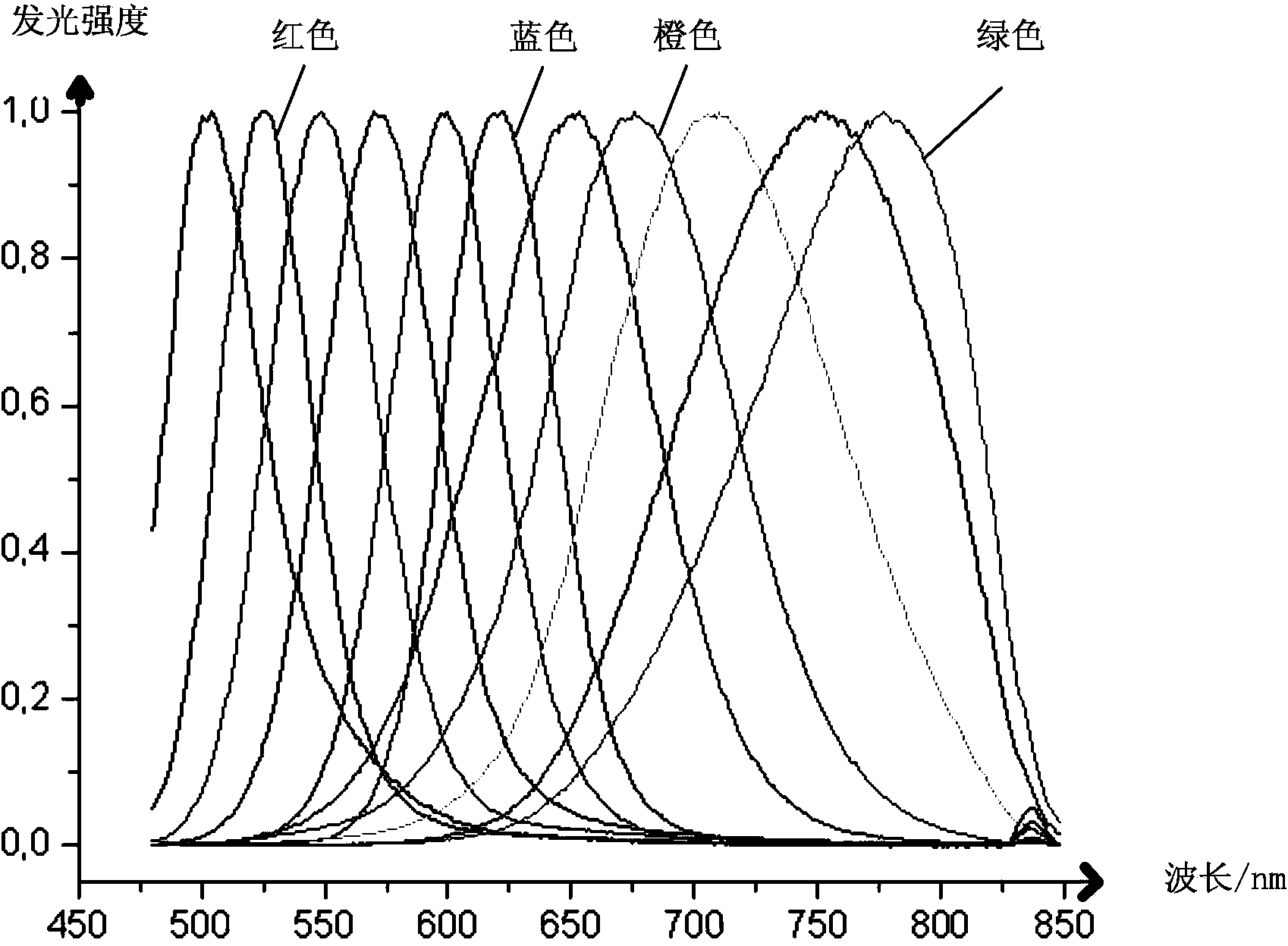
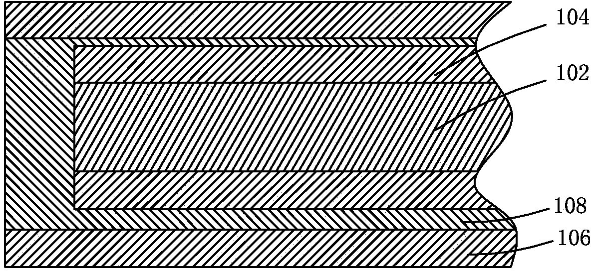
[0042] see Figure 8 to Figure 10 , the present invention provides an LED package, which can be applied to the backlight module in the field of display technology, which specifically includes: a first support 10, several LED elements 20, encapsulation glue 30 and quantum strips 40, the first support 10 includes a PCB board 12 and four side walls 14 formed on the peripheral edge of the PCB board 12, and the four side walls 14 enclose an accommodating space 18, and the plurality of LED elements 20 are mounted on the On the PCB board 12 and located in the accommodating space 18, and electrically connected with the PCB board 12, the packaging glue 30 is filled in the accommodating space 18, and the upper ends of the four side walls 14 are all A m...


PUM


Abstract

The invention provides an LED packaged piece and a manufacturing method of the LED packaged piece. The LED packaged piece comprises a first support (10), a plurality of LED elements (20), a packaging adhesive (30) and a quantum dot bar (40). The first support (10) comprises a PCB (12) and four side walls (14) defining an accommodating space (18). The LED elements (20) are installed on the PCB (12) and are electrically connected with the PCB (12). The packaging adhesive (30) is filled into the accommodating space (18). Four installing parts (16) are arranged at the upper ends of the four side walls (14) respectively, and the quantum dot bar (40) is installed on the installing parts (16) and located above the packaging adhesive (30). The first support (10), the LED elements (20) and the quantum dot bar (40) are integrally packaged so as to be fixedly combined together.

Description

technical field [0001] The invention relates to the technical field of LED (Light Emitting Diode, light emitting diode) packaging, in particular to an LED package with a quantum device and a manufacturing method thereof. Background technique [0002] Quantum Dots (QuantumDots, QD), also known as nanocrystals, are composed of a limited number of atoms, and the three dimensions are all on the order of nanometers. see figure 1 , Quantum dots are generally spherical or quasi-spherical, and are nanoparticles made of semiconductor materials (usually composed of II-VI or III-V elements) with stable diameters between 1-10nm. Quantum dots are aggregates of atoms and molecules on the nanometer scale, which can be composed of a semiconductor material, such as group II and VI elements (such as CdS, CdSe, CdTe, ZnSe, etc.) or group III and V elements (such as InP , InAs, etc.), can also be composed of two or more semiconductor materials. [0003] Quantum dots are semiconductor nanostr...

Claims


Application Information

Patent Timeline
Patent Type & Authority Applications(China)
IPC IPC(8): H01L33/00H01L33/58H01L33/54H01L33/48
CPCH01L25/0753H01L33/52H01L2933/0033H01L33/501H01L33/502H01L33/505H01L2933/0041H01L33/002H01L33/005H01L33/04H01L33/48H01L33/483H01L2924/12041H01L27/15H01L2933/005
Inventor 丘永元康志聪张简圣哲苏赞加
Owner TCL CHINA STAR OPTOELECTRONICS TECH CO LTD
Why Eureka
Try Eureka