Pixel unit, array substrate and display panel

An array substrate, pixel unit technology, applied in electrical components, optics, instruments, etc., can solve the problem of small aperture ratio of pixel units, and achieve the effect of increasing the aperture ratio and the coverage area.

Inactive Publication Date: 2014-04-09
TRULY SEMICON
View PDF6 Cites 14 Cited by
  • Summary
  • Abstract
  • Description
  • Claims
  • Application Information

AI Technical Summary

Problems solved by technology

The aperture ratio of existing pixel units is small

Method used


Image

  • Pixel unit, array substrate and display panel
  • Pixel unit, array substrate and display panel
  • Pixel unit, array substrate and display panel

Examples


Embodiment Construction

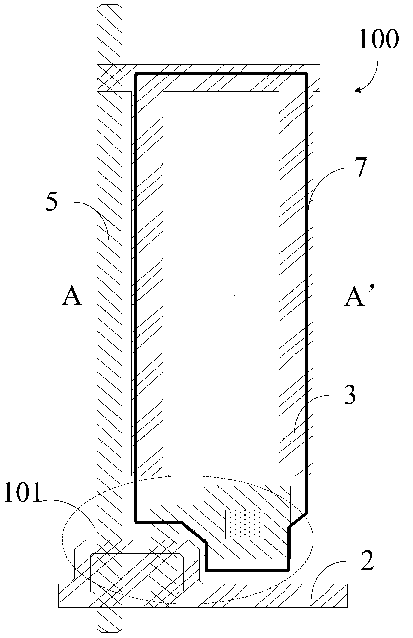
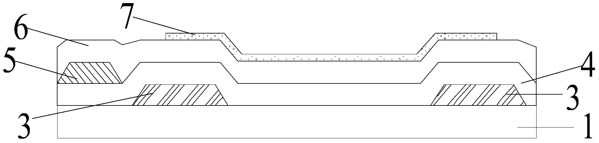
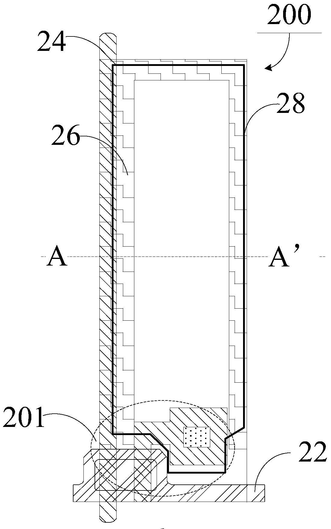
[0023] As mentioned in the background art, the existing pixel unit has a small aperture ratio. The inventor found that the cause of this defect is mainly due to the fact that in the existing pixel unit, there are common electrode lines, data lines and pixel electrode lines in sequence from the light transmission direction of the pixel unit, because the data lines interfere with the pixel electrode lines, so The pixel electrode lines cannot extend outward, let alone cover the data lines, so the coverage area of ​​the pixel electrodes is small, which limits the aperture ratio of the pixel unit.

[0024] Based on this, the present invention provides a pixel unit, which is applied to an array substrate, including a transparent substrate, and a common electrode line, a data line, and a pixel electrode located on the transparent substrate, wherein the common electrode line is located on the conductive line where the data line is located. layer and the conductive layer where the pixe...


PUM


Abstract

The invention discloses a pixel unit, an array substrate and a display panel. A public electrode wire is formed between a conductive layer where a pixel electrode is located and a conductive layer where a data line is located and a covering zone of the public electrode wire comprises a zone where the data line is located. Due to the fact that a public electrode has the shielding function, the electric field action of the data line does not need to be considered according to the pixel electrode, the pixel electrode can extend outwards to the position close to the data line, the covering zone of the pixel electrode is increased, and the aperture ratio of the pixel unit is increased.

Description

technical field [0001] The present invention relates to the field of display technology, and more specifically, to a pixel unit, an array substrate and a display panel. Background technique [0002] As one of the components of the display panel, the array substrate is of great significance. refer to Figure 1a and 1b As shown, the array substrate includes a plurality of pixel units 100 , and the pixel units 100 include thin film field effect transistors 101 . [0003] Wherein, the pixel unit 100 includes a transparent substrate 1 along the section AA' of the pixel unit 100; a first conductive layer is formed on the surface of the transparent substrate 1, and the first conductive layer includes gate lines 2, common electrode lines 3 and The gate of the thin film field effect transistor 101, the gate line 2 is connected to the gate of the thin film field effect transistor 101; the first insulating layer 4 covering the first conductive layer; the second conductive layer forme...

Claims


Application Information

Patent Timeline
Patent Type & Authority Applications(China)
IPC IPC(8): H01L27/12H01L23/50G02F1/1362G02F1/1368G02F1/1343
Inventor 庄崇营胡君文李林洪胜宝何基强李建华
Owner TRULY SEMICON
Why Eureka
Try Eureka