Liquid crystal display device with in-plane switching mode

A liquid crystal display device and liquid crystal technology, applied in static indicators, nonlinear optics, instruments, etc., can solve problems such as inability to control the inclination angle of the liquid crystal layer, deteriorate the flickering display of the liquid crystal display device, etc., achieve improved contrast, realize viewing angle characteristics, eliminate The effect of viewing angle properties

Active Publication Date: 2017-12-15
TIANMA MICRO ELECTRONICS CO LTD
View PDF2 Cites 0 Cited by
  • Summary
  • Abstract
  • Description
  • Claims
  • Application Information

AI Technical Summary

Problems solved by technology

Although it is necessary to increase the electric field perpendicular to the substrate to control the tilt angle of the liquid crystal molecules, the electric field will deteriorate the flickering display of the liquid crystal display device
[0025] In the technique of Japanese Patent Laid-Open No. 2001-091974 (Patent Document 2), liquid crystal molecules are moved in a direction perpendicular to the substrate between the signal line and the pixel electrode (or common electrode) at the outer side of the pixel. region, the inclination angle of the liquid crystal layer in the region through which the light in the pixel passes cannot be controlled

Method used


Image

  • Liquid crystal display device with in-plane switching mode
  • Liquid crystal display device with in-plane switching mode
  • Liquid crystal display device with in-plane switching mode

Examples


example 1

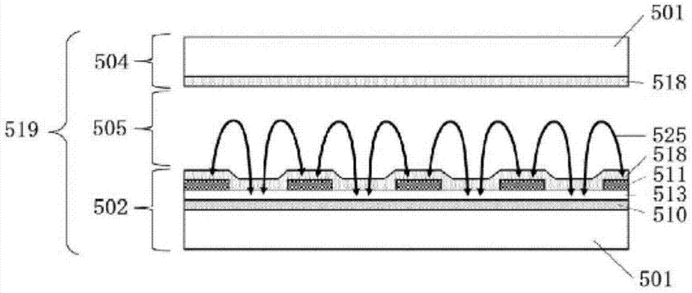
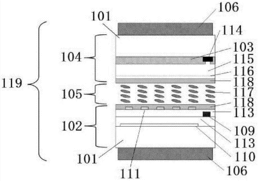
[0062] Such as image 3 As shown, in the liquid crystal display device in this embodiment mode, the TFT substrate 102 and the color filter substrate 104 are close to each other at a certain interval, the transistors (not shown) in the TFT substrate 102 are formed on the glass substrate 101, and the color filter substrate 104 is formed on the glass substrate 101. The color layer 103 and the like in the optical sheet substrate 104 are similarly formed on the glass substrate 101, and the liquid crystal layer 105 is sealed between the two substrates. Polarizing plates 106 are placed on the outer sides of the TFT substrate 102 and the color filter substrate 104 .

[0063] Figure 4 A plan view of a pixel of the TFT substrate 102 is shown. Wiring of gate lines 107 , common electrode lines 108 , and signal lines 109 is formed on the TFT substrate 102 of the liquid crystal display device of the present embodiment. Omitted in the drawing, the gate lines 107 are plural on the TFT sub...

example 2

[0092] Figure 12 A plan view showing a pixel of a liquid crystal display device according to Example 2 of the present invention. Figure 13 It is a cross-sectional view showing the operation when black is displayed in the liquid crystal display device according to Example 2 of the present invention.

[0093] As in the case of the liquid crystal display device of Example 1, on the TFT substrate 202 of the liquid crystal display device of Example 2 of the present invention, wirings of gate lines 207, common electrode lines 208, and signal lines 209 are formed. As omitted in the drawing, the gate lines 207 are plural on the TFT substrate and placed parallel to each other. The common electrode lines 208 and the signal lines 209 are similarly also plural and respectively placed parallel to each other. In addition, gate lines 207, common electrode lines 208, and signal lines 209 are extended to the periphery of the TFT substrate 202, and are all connected to an external power sou...

example 3

[0101] A liquid crystal display device according to Example 3 of the present invention is a modification for driving the liquid crystal display device according to Example 1 of the present invention, and has an electric field control section for forming an alternating electric field different from that of the liquid crystal display device according to Example 1. Electric field control components.

[0102] In addition, configurations in this example that are the same as those in Example 1 are also marked with reference symbols whose last two digits are the same as those in Example 1.

[0103] FIG. 14 indicates respective electrode potentials of the liquid crystal display device according to the present Example 3. FIG. In Example 3, an alternating electric field is formed by periodically changing the potentials of the CF-side common electrode 316 and the TFT-side common electrode 310 in opposite directions.

[0104] In Example 3 of the present invention, each amplitude width of...


PUM


Abstract

A liquid crystal display device according to the present invention is directed at optimizing the viewing angle characteristics of black luminance in a diagonal direction by realizing a low tilt angle without depending on an oriented film or an orientation treatment method in an FFS mode. The liquid crystal display device of the present invention is a liquid crystal display device in the FFS mode, including: a liquid crystal layer having a negative dielectric anisotropy; a color filter substrate disposed to sandwich the liquid crystal layer; and a TFT substrate having pixels, wherein a CF side common electrode which controls a potential is present in a liquid crystal layer side of the color filter substrate; and there is electric field controlling means which forms an alternating electric field between the CF side common electrode and a TFT side common electrode.

Description

technical field [0001] The present invention relates to a liquid crystal display device, in particular, the liquid crystal display device is improved in viewing angle characteristics with respect to a tilt angle by using fringing field switching (FFS) technology, and the liquid crystal display device has wide viewing angle characteristics. Background technique [0002] Liquid crystal display devices have been used in various displays of computers, televisions, etc., because of their outstanding characteristics of small thickness, light weight, and low power consumption. [0003] There are various operation modes for the liquid crystal display panel of the liquid crystal display device. Examples of these operation modes are: Twisted Nematic (TN) mode, In-Plane Switching (IPS) mode, FFS mode, and the like. In TN mode, the liquid crystal molecules between two glass substrates are twisted and oriented; in IPS mode, a transverse electric field is applied through a pair of electr...

Claims


Application Information

Patent Timeline
Patent Type & Authority Patents(China)
IPC IPC(8): G02F1/1343
CPCG02F1/134363G09G3/3655G09G2300/0434G02F1/133749G02F1/134372G02F1/134381G02F1/13712
Inventor 恩田真也池野英德
Owner TIANMA MICRO ELECTRONICS CO LTD
Why Eureka
Try Eureka