
Transverse power device with super junction structure and manufacturing method thereof

A technology for lateral power devices and manufacturing methods, applied in semiconductor/solid-state device manufacturing, semiconductor devices, electrical components, etc., can solve problems such as substrate auxiliary depletion, avoid charge imbalance, and suppress substrate auxiliary depletion effect of effect

Inactive Publication Date: 2014-04-23
SHANGHAI SIMGUI TECH
View PDF5 Cites 0 Cited by
  • Summary
  • Abstract
  • Description
  • Claims
  • Application Information

AI Technical Summary

Problems solved by technology

[0006] The disadvantage of the above-mentioned superjunction structure used in lateral devices is that the substrate participates in the depletion of the superjunction column region, which leads to the substrate-assisted depletion effect

Method used


Image

  • Transverse power device with super junction structure and manufacturing method thereof
  • Transverse power device with super junction structure and manufacturing method thereof
  • Transverse power device with super junction structure and manufacturing method thereof

Examples


Embodiment Construction

[0021] The specific implementation of the lateral power device with super junction structure and the manufacturing method provided by the present invention will be described in detail below with reference to the accompanying drawings.

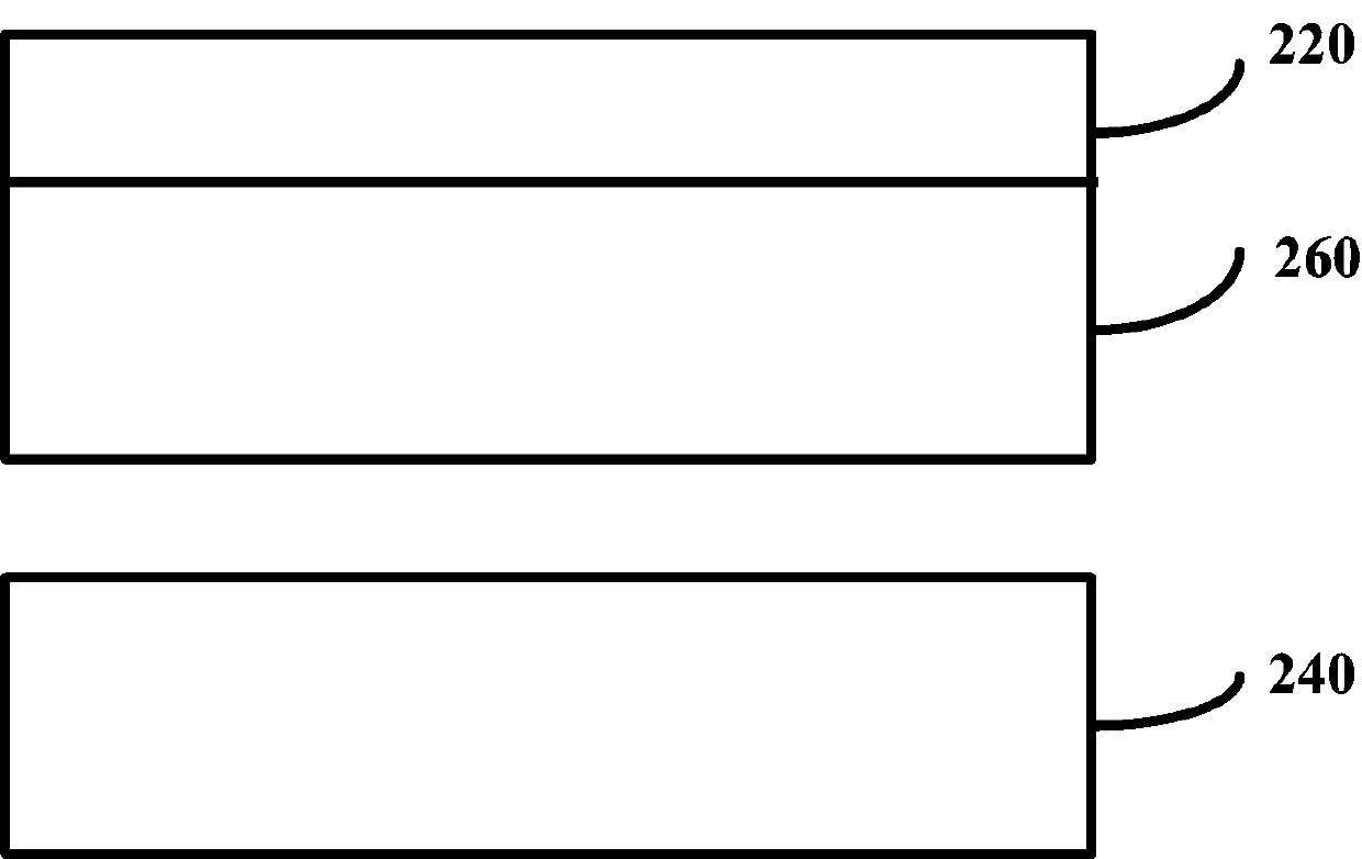
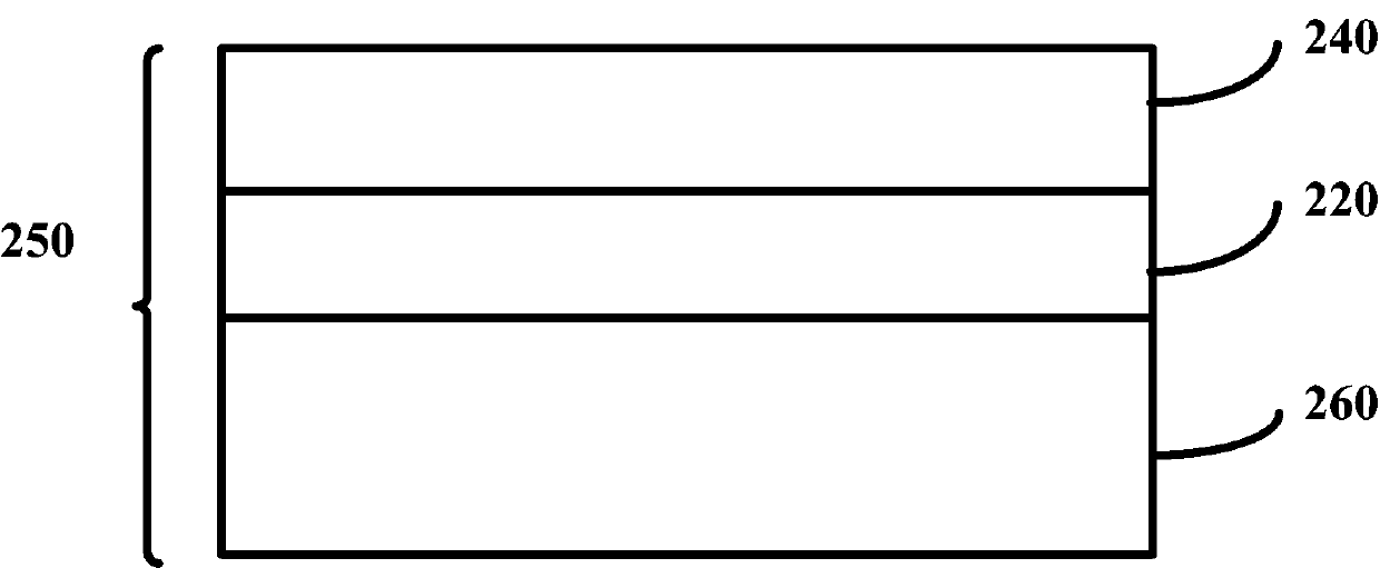
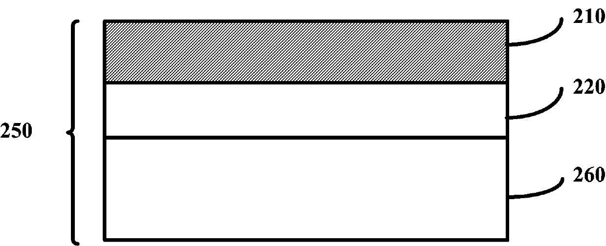
[0022] Reference attached figure 2 Shown is a schematic diagram of a lateral power device with a super junction structure described in this specific embodiment, including a P-type support substrate 200, a silicon germanium layer 210 located on the surface of the support substrate, and a silicon germanium layer located on the surface of the silicon germanium layer. The buried oxide layer 220 and the active layer 230 located on the surface of the buried oxide layer; the active layer includes a gate region 234, a source region 233 and a drain region 237 respectively located on both sides of the gate region 234 and a The drift region between the region 234 and the drain region 237; the source region 233 and the drain region 237 are both N-type dop...


PUM


Abstract

The invention provides a transverse power device with a super junction structure and a manufacturing method thereof. The transverse power device with the super junction structure comprises a support substrate, a germanium silicon layer, an insulating buried layer and an active layer, wherein the germanium silicon layer is positioned on the surface of the support substrate, the insulating buried layer is positioned on the surface of the germanium silicon layer, the active layer is positioned on the surface of the insulating buried layer and comprises a grid region, a source region, a drain region and a drift region, the source region and the drain region are respectively positioned at two sides of the grid region, and the drift region is positioned between the grid region and the drain region and comprises a plurality of doped regions with a first conduction type and a plurality of doped regions with a second conduction type, which are arranged in a transverse alternate contact mode. The transverse power device and the manufacturing method have the advantages that through the existence of the germanium silicon layer arranged under the insulating buried layer, the auxiliary depletion effect of the substrate can be greatly inhibited, and the advanced breakdown caused by the charge unbalance of the shift region is avoided.

Description

technical field [0001] The invention relates to a lateral power device with a super-junction structure and a manufacturing method, in particular to a super-junction lateral power device and a manufacturing method that suppresses the substrate-assisted depletion effect, and belongs to the technical field of microelectronics and solid electronics. Background technique [0002] Power integrated circuits are sometimes called high-voltage integrated circuits, which are an important branch of modern electronics. They can provide new circuits with high speed, high integration, low power consumption and radiation resistance for various power conversion and energy processing devices, and are widely used in electric power Daily consumption fields such as control systems, automotive electronics, display device drivers, communications and lighting, as well as many important fields such as national defense and aerospace. The rapid expansion of its application scope has also put forward h...

Claims


Application Information

Patent Timeline
IPC IPC(8): H01L29/78H01L29/06H01L21/336
CPCH01L29/7816H01L29/063H01L29/66681
Inventor 魏星夏超狄增峰方子韦
Owner SHANGHAI SIMGUI TECH
Features
  • Generate Ideas
  • Intellectual Property
  • Life Sciences
  • Materials
  • Tech Scout
  • Unparalleled Data Quality
  • Higher Quality Content
  • 60% Fewer Hallucinations
Learn More