Power semiconductor device
A power semiconductor and semiconductor technology, applied in semiconductor devices, electrical components, circuits, etc., can solve the problems of charge imbalance and lower breakdown voltage of power semiconductor devices, and achieve the effect of avoiding charge imbalance and improving breakdown voltage.
- Summary
- Abstract
- Description
- Claims
- Application Information
AI Technical Summary
Problems solved by technology
Method used
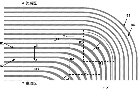
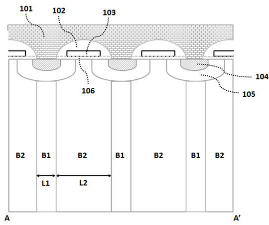
Image

Examples
Embodiment Construction
[0017] It should be noted that, in the case of no conflict, the embodiments of the present invention and the features in the embodiments can be combined with each other. The present invention will be described in detail below with reference to the accompanying drawings and examples.
[0018] In order to enable those skilled in the art to better understand the solutions of the present invention, the following will clearly and completely describe the technical solutions in the embodiments of the present invention in conjunction with the accompanying drawings in the embodiments of the present invention. Obviously, the described embodiments are only Embodiments of some, but not all, embodiments of the present invention. Based on the embodiments of the present invention, all other embodiments obtained by persons of ordinary skill in the art without creative efforts shall fall within the protection scope of the present invention.
[0019] It should be noted that the terms "first" a...
PUM
 Abstract
Description
Claims
Application Information
PatSnap Eureka turns technology decisions into work you can execute. Powered by our Innovation Knowledge Graph, it runs expert workflows across engineering, life sciences, materials and intellectual property. Get your review-ready output in minutes.


