Method using non Forster circuit high frequency response to carry out broadband impedance matching

A frequency response and impedance matching technology, applied in impedance matching network, multi-terminal pair network, etc., can solve the problems of bandwidth limitation and difficulty in breaking through the frequency bottleneck.

Inactive Publication Date: 2014-05-07
ZHEJIANG UNIV
View PDF2 Cites 10 Cited by
  • Summary
  • Abstract
  • Description
  • Claims
  • Application Information

AI Technical Summary

Problems solved by technology

At present, many applications are limited by the bandwidth of the negative impedance transformation circuit, and only non-Foster devices within 500MHz can be real

Method used


Image

  • Method using non Forster circuit high frequency response to carry out broadband impedance matching
  • Method using non Forster circuit high frequency response to carry out broadband impedance matching
  • Method using non Forster circuit high frequency response to carry out broadband impedance matching

Examples


Embodiment Construction

[0016] The present invention will be further described below in conjunction with the accompanying drawings and embodiments.

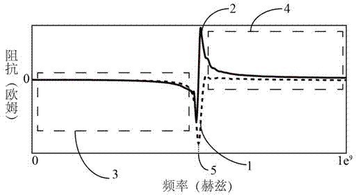
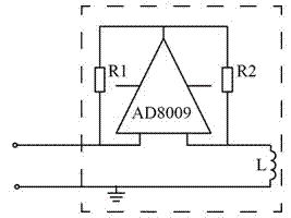
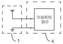
[0017] Such as image 3 , Figure 5 As shown, the present invention connects the electrically small-sized antenna 7 with the non-Foster module 6, utilizes the negative reactance characteristic on the right side of the frequency response resonance point 5 of the non-Foster module frequency response, and compensates the height of the electrically small-sized antenna 7. Frequency reactance, to achieve the purpose of broadband impedance matching at high frequencies.

[0018] The high-frequency reactance compensation method of the electrically small-sized antenna 7 is as follows: the impedance of the electrically small-sized antenna 7 is equivalent to a capacitance, and at high frequencies, the reactance curve of the electrically small-sized antenna 7 is on the right side of the resonance point of the frequency response of the non-FOSS module. The negative...


PUM


Abstract

The invention discloses a method using non Forster circuit high frequency response to carry out broadband impedance matching. An electrically small size antenna is connected with a non Forster module. The negative reactance characteristic on the right side of a non Forster module frequency response resonant point is used to compensate the high frequency reactance of the electrically small size antenna, so as to realize broadband impedance matching at a high frequency position. When the traditional non Forster module is applied to the electrically small size antenna, reactance compensation is carried out simply through low frequency response, which has the defect that broadband impedance matching cannot be realized in high frequency. According to the invention, a negative reactance region on the right side of the non Forster module frequency response resonant point is used to realize reactance compensation of the electrically small size antenna, and high frequency broadband matching is realized.

Description

technical field [0001] The invention relates to a method for performing broadband impedance matching by utilizing the high-frequency frequency response of a non-Foster circuit. Background technique [0002] With the widespread application of advanced communication technologies such as frequency modulation and spread spectrum, the development of large-scale integrated circuits and space technology, and the miniaturization of electronic devices, higher requirements are placed on the miniaturization of communication equipment and system bandwidth. As a key component in communication equipment, the antenna is a converter of electromagnetic energy from the equipment to the space, and its performance directly affects the working quality of the equipment. Therefore, the research on the miniaturization and bandwidth of the antenna has always been a research in this field. hotspot. [0003] In recent years, research results on non-Foster devices have shown that in the microwave fiel...

Claims


Application Information

Patent Timeline
IPC IPC(8): H03H11/28
Inventor 杨婧茹冉立新
Owner ZHEJIANG UNIV
Why Eureka
Try Eureka