

Optical semiconductor element, method for controlling optical semiconductor element, and method for manufacturing optical semiconductor element
A technology of optical semiconductor components and control methods, applied in optical components, light guides, optics, etc., can solve the problems of compromise between wavelength bandwidth and modulation efficiency, narrowing of wavelength bandwidth, and difficulty in achieving stable control.
- Summary
- Abstract
- Description
- Claims
- Application Information
AI Technical Summary
Problems solved by technology
Method used
Image

Examples
no. 1 Embodiment approach )
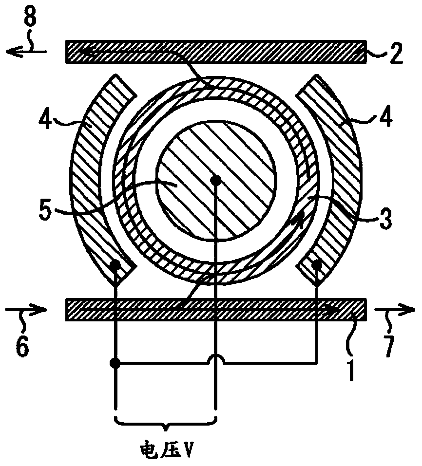
[0063] First, the first embodiment will be described. Figure 1A is a diagram showing an example of a ring modulator. This ring modulator includes two linear waveguides 1 and 2 and a ring waveguide 3 provided therebetween. In addition, the modulation electrode 4 is provided outside the ring waveguide 3 , and the modulation electrode 5 is provided inside the ring waveguide 3 .
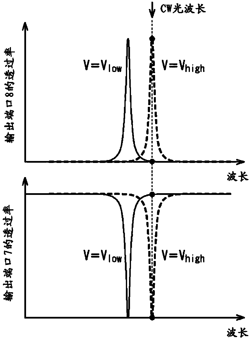
[0064] Furthermore, when the CW light incident on the input port 6 of the waveguide 1 coincides with the wavelength of the CW light at the ring resonance wavelength (an integer fraction of the optical path length of the circular waveguide 3) determined by the optical path length of the optical revolution of the ring waveguide 3, is introduced into the output port 8 of the waveguide 2 . On the other hand, when the ring resonance wavelength does not match the wavelength of the CW light, it is introduced into the output port 7 of the waveguide 1 . In addition, when the modulation voltage V applied to the...
no. 2 Embodiment approach )
[0075] Next, a second embodiment will be described. Figure 10A is a diagram showing the layout of the optical semiconductor element according to the second embodiment, Figure 10B is along Figure 10A A cross-sectional view of the line I-II, Figure 10C is along Figure 10A Sectional view of line III-II.
[0076] In the second embodiment, if Figure 10B as well as Figure 10C As shown, SiO is formed on the Si substrate 101 2 Film 102. And, if Figure 10A ~ Figure 10C shown in SiO 2 On membrane 102, the annular n + layer 105n, n - layer 104n,p - Layer 104p and p + The layers 105p are arranged in this order from the inner side and formed. in n + layer 105n, n - layer 104n,p - Layer 104p and p + The layer 105p uses, for example, Si doped with impurities. Additionally, covering n + layer 105n, n - layer 104n, p-layer 104p and p + SiO of layer 105p 2 film 106 formed on SiO 2 film 102, the SiO 2 film 106 and n - layer 104n and p - A ring-shaped heater 107 is...
no. 3 Embodiment approach )
[0084] Next, a third embodiment will be described. Figure 11A is a diagram showing the layout of the optical semiconductor element according to the third embodiment, Figure 11B is along Figure 11A A cross-sectional view of the line I-II, Figure 11C is along Figure 11A Sectional view of line III-II.
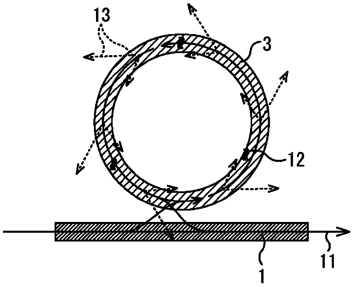
[0085] In the third embodiment, if Figure 11A ~ Figure 11C shown, in n + The inner side of the layer 105n is provided with a ring-shaped light absorbing material 114b, and the inner side is also provided with a groove 115. Other configurations are the same as those of the second embodiment.
[0086] In such a third embodiment, absorption of light 131 and heat generation 132 also occur in the light-absorbing material 114b. Therefore, heat can be used more efficiently than in the second embodiment.
[0087] In addition, if the light-absorbing material 114b is provided, the light-absorbing material 114a may not be provided.
PUM
 Abstract
Description
Claims
Application Information