Anisotropic conductive film, composition for same, and semiconductor device

An anisotropic, conductive film technology, used in semiconductor devices, conductive adhesives, conductive materials dispersed in non-conductive inorganic materials, etc., can solve problems such as the operation of bonding failure equipment, the inability of bonding equipment to reach the bonding temperature, etc., Achieving the effect of low adhesion strength reduction rate, excellent adhesion and connection reliability, and low connection resistance growth rate

Active Publication Date: 2017-01-04
KUKDO ADVANCED MATERIALS CO LTD
View PDF16 Cites 0 Cited by
  • Summary
  • Abstract
  • Description
  • Claims
  • Application Information

AI Technical Summary

Problems solved by technology

However, such an anisotropic conductive adhesive is used as an adhesive for bonding at a high temperature of 180°C or higher, and thus suffers from bonding failure or problems regarding device operation
[0005] In addition, even when the effective temperature of the bonding equipment is raised as much as possible, the bonding equipment sometimes cannot reach the desired bonding temperature according to the type of PCB.

Method used


Image

  • Anisotropic conductive film, composition for same, and semiconductor device
  • Anisotropic conductive film, composition for same, and semiconductor device
  • Anisotropic conductive film, composition for same, and semiconductor device

Examples


Embodiment 1 to 3

[0085] Examples 1 to 3: Preparation of anisotropic conductive composition and anisotropic conductive film

[0086] Acrylonitrile butadiene copolymer, acrylate-modified urethane resins 1 and 2, acryl-based copolymer, free radical polymerizable material 1 and 2, organic peroxide were blended in the amounts listed in Table 1. material, titanium dioxide, silicon dioxide, and conductive particles, and then stirred with a planetary mixer at 25° C. for 60 minutes while preventing the conductive particles from being pulverized. The resulting mixture was coated on a polyethylene-based film treated with a silicone release surface to form a film with a thickness of 35 μm. Each of the anisotropic conductive films of Examples 1 to 3 was prepared by forming a film using a casting blade and then drying at 60° C. for 5 minutes.

experiment example

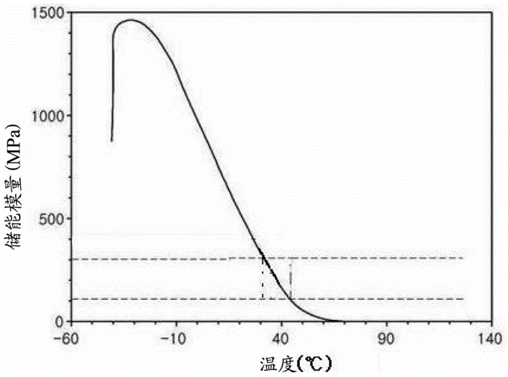
[0103] Experimental example: Measurement of storage modulus at 40°C, initial adhesive strength, initial connection resistance, and connection resistance after reliability testing

[0104] The storage modulus at 40° C., initial adhesive strength, initial connection resistance, and connection resistance after the reliability test of the anisotropic conductive films prepared in Examples and Comparative Examples were measured as follows.

[0105] (1) Storage modulus at 40°C

[0106] A 35 μm thick anisotropic conductive film was placed on a heat press, and a 0.2 mm thick silicone rubber was placed on the film, and heated and compressed at 190 °C and 30 MPa for 15 minutes to cure the above connection material, and then the release Type film.

[0107] Then, the storage modulus of the film at 40° C. was measured using a dynamic mechanical analyzer (DMA) (TA Instruments) while heating from −40° C. to 200° C. at a rate of 10° C. / min.

[0108] (2) Initial adhesive strength and initial ...


PUM

PropertyMeasurementUnit
storage modulusaaaaaaaaaa

Abstract

A semiconductor device connected by an anisotropic conductive film, the film having a storage modulus of 100 MPa to 300 MPa at 40° C. after curing of the film, and a peak point of 80° C. to 90° C. in a DSC (Differential Scanning calorimeter) profile of the film.

Description

technical field [0001] The present invention relates to a composition for an anisotropic conductive film and an anisotropic conductive film produced using the composition. Background technique [0002] Anisotropic conductive films are materials used to electrically connect small electrical components such as semiconductor devices to substrates or to electrically connect substrates to each other in the manufacture of electronic products such as liquid crystal displays, personal computers, and mobile communication devices. [0003] With the recent trend toward large panels and fine interconnect lines, the connection substrate becomes thinner, and the distance between the circuit connection part and the chip, multilayer ceramic chip (MLCC) or via hole, etc. decreases, causing severe temperature deviation . In addition, the heat dissipation of each pattern of the printed circuit board (PCB) also causes temperature deviation. [0004] Conventional anisotropic conductive films h...

Claims


Application Information

Patent Timeline
Patent Type & Authority Patents(China)
IPC IPC(8): H01B5/00H01B1/22H01L23/488C09J7/02C09J9/02C09J175/14C09J133/00C09J11/04
CPCH01L24/29H01L24/27H01L24/32H01L24/83H01L2224/27502H01L2224/2784H01L2224/29082H01L2224/2929H01L2224/29291H01L2224/29311H01L2224/29316H01L2224/29324H01L2224/29339H01L2224/29344H01L2224/29347H01L2224/29355H01L2224/29364H01L2224/29366H01L2224/29371H01L2224/29386H01L2224/2939H01L2224/29393H01L2224/294H01L2224/2949H01L2224/29499H01L2224/32225H01L2224/73204H01L2224/83101H01L2224/83855H01L2224/8388H01L2224/83885H01L2924/07811H01L2924/20104H01L2924/20105
Inventor 申炅勋金奎峰徐贤柱申颍株林佑俊
Owner KUKDO ADVANCED MATERIALS CO LTD
Why Eureka
Try Eureka