Semiconductor device

A semiconductor and transistor technology, applied in the field of semiconductor devices, can solve the problem of increasing the area of ​​semiconductor devices, achieve the effect of reducing the area and suppressing the latch-up effect

Active Publication Date: 2018-02-09
SII SEMICONDUCTOR CORP
View PDF4 Cites 0 Cited by
  • Summary
  • Abstract
  • Description
  • Claims
  • Application Information

AI Technical Summary

Problems solved by technology

[0005] However, in the technology disclosed in Patent Document 1, the P-type diffusion region 82 in the direction from the ESD protection circuit toward the internal circuit is long in the horizontal direction, and accordingly, the area of ​​the semiconductor device increases.

Method used


Image

  • Semiconductor device
  • Semiconductor device
  • Semiconductor device

Examples


Embodiment Construction

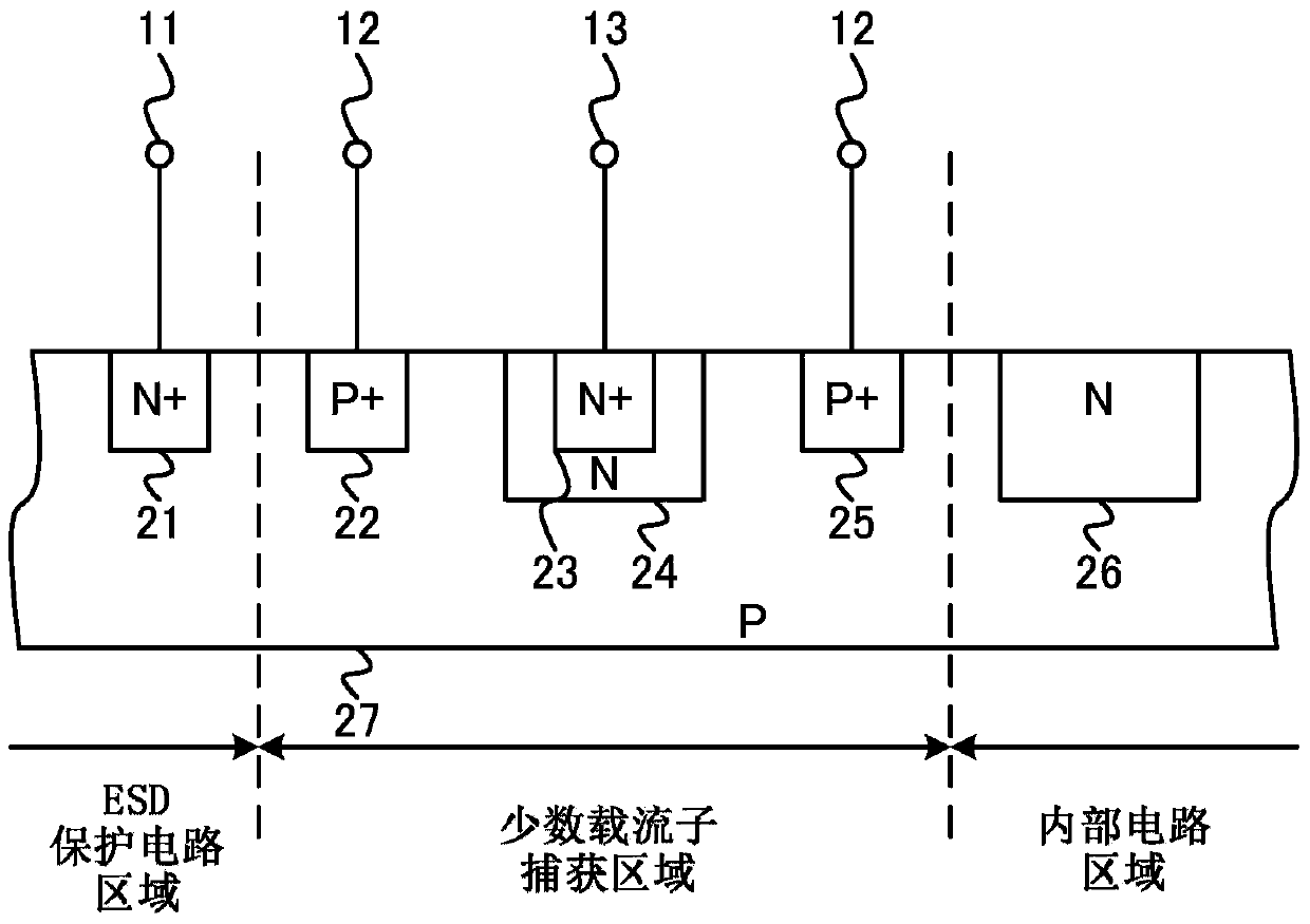
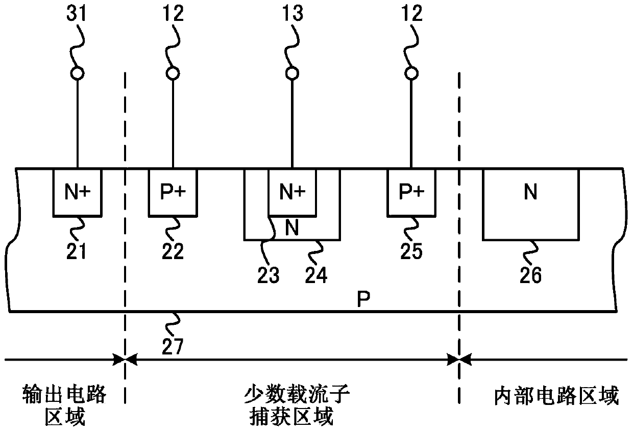
[0025] Hereinafter, embodiments of the present invention will be described with reference to the drawings. First, the structure of the semiconductor device will be described. figure 1 is a cross-sectional view showing a semiconductor device, figure 2 It is a top view showing a semiconductor device.

[0026] Such as figure 1 As shown, the semiconductor substrate 27 is composed of three regions, the ESD protection circuit region, the internal circuit region and the minority carrier trapping region. The ESD protection circuit region is used to protect the semiconductor device from the influence of ESD, and the minority carrier The carrier trapping region traps minority carriers generated in the semiconductor substrate 27 due to a surge having a negative voltage applied to the pad 11 of the input or output, the minority carrier trapping region surrounds the internal circuit area, usually forming a protective ring. The input or output pad 11, the ground pad 12, the power pad...


PUM


Abstract

The present invention provides a semiconductor device capable of suppressing the occurrence of latch-up effect with a small area. In the minority carrier trapping region, a P-type diffusion region (22), an N-type well (24) and a P-type diffusion region (25) are formed on the surface of a P-type semiconductor substrate (27). The N-type diffusion region (23) is formed on the surface of the N-type well (24). At this time, the N-type well (24) is sandwiched between the P-type diffusion region (22) and the P-type diffusion region (25). The P-type diffusion region ( 22 ) and the P-type diffusion region ( 25 ) are not connected by the shortest distance, but are connected by metal film wiring arranged in a detour, and both are connected to the ground pad ( 12 ).

Description

technical field [0001] The present invention relates to semiconductor devices. More specifically, it relates to a semiconductor device capable of suppressing the occurrence of latch-up. Background technique [0002] First, a conventional semiconductor device will be described. Figure 5 It is a sectional view showing a conventional semiconductor device. [0003] When a surge with a negative voltage is applied to the input pad 71, electrons as minority carriers in the P-type semiconductor substrate 87 sometimes leak from the N-type diffusion region 81 in the ESD protection circuit region to the P-type semiconductor substrate 87 . The minority carriers flow from the semiconductor substrate 87 into the P-type diffusion region 82 connected to the ground pad 72 to be absorbed. Here, the length of the P-type diffusion region 82 in the horizontal direction in the direction from the ESD protection circuit toward the internal circuit is long enough so that minority carriers are su...

Claims


Application Information

Patent Timeline
Patent Type & Authority Patents(China)
IPC IPC(8): H01L27/02
CPCH01L21/761H01L27/0255H01L27/0921H01L23/60
Inventor 樱井仁美广濑嘉胤
Owner SII SEMICONDUCTOR CORP
Why Eureka
Try Eureka