
ESD protection circuit based on CMOS technology and structure thereof

A technology for protecting circuits and structures, applied in circuits, electrical components, electrical solid devices, etc., to solve problems such as electronic equipment failures or malfunctions, component aging, and electromagnetic interference.

Active Publication Date: 2017-11-07
SHENZHEN YSPRING TECH
View PDF5 Cites 0 Cited by
  • Summary
  • Abstract
  • Description
  • Claims
  • Application Information

AI Technical Summary

Problems solved by technology

At this stage, when the electrostatic protection capability of ESD in the low-power CMOS process is lower than 3000V, it is easy to cause failure or malfunction of electronic equipment, resulting in electromagnetic interference; it will also break down integrated circuits and precision electronic components, resulting in aging of components and reducing production Yield

Method used


Image

  • ESD protection circuit based on CMOS technology and structure thereof
  • ESD protection circuit based on CMOS technology and structure thereof
  • ESD protection circuit based on CMOS technology and structure thereof

Examples


Embodiment Construction

[0027] It should be noted that, in the case of no conflict, the embodiments in the present application and the features in the embodiments can be combined with each other.

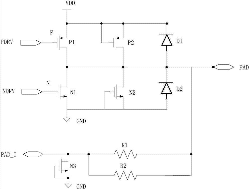
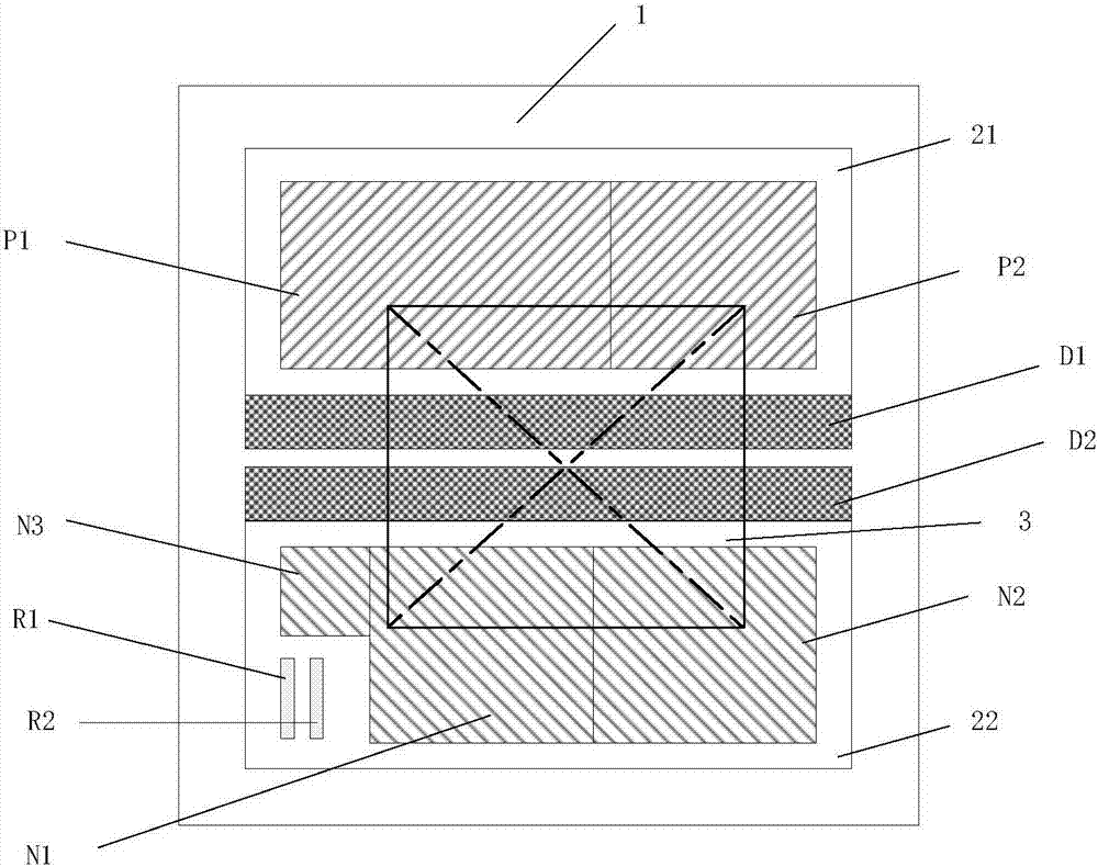
[0028] figure 1It is a schematic block diagram of an ESD electrostatic protection circuit based on a CMOS process of the present invention, figure 2 It is an ESD electrostatic protection circuit diagram based on CMOS technology of the present invention, combined with figure 1 and figure 2 , an ESD protection circuit based on CMOS technology, including a pre-driver terminal, a drive tube, a protection circuit, an input / output interface terminal and an internal signal terminal, the output terminal of the pre-driver terminal is connected to the input terminal of the drive tube, and the output terminal of the drive tube It is connected with the input end of the protection circuit, the output end of the protection circuit is connected with the input / output interface end, and the internal signal end is conne...


PUM


Abstract

The invention discloses an ESD protection circuit based on a CMOS technology. The circuit comprises a predriving terminal, a driving pipe, a protection circuit, an input / output interface terminal and an internal signal terminal. An output terminal of the predriving terminal is connected to an input terminal of the driving pipe. An output terminal of the driving pipe is connected to an input terminal of the protection circuit. An output terminal of the protection circuit is connected to the input / output interface terminal. The internal signal terminal is connected to the input / output interface terminal through connecting the protection circuit. The invention also discloses an ESD protection structure based on the CMOS technology. The structure comprises a substrate, a well region, a transistor, a diode, a resistor and a PAD layer. The invention relates to the integrated circuit technology field. By using the ESD protection circuit based on the CMOS technology and the structure thereof, the diode in the protection circuit is inversely connected to a power supply; reverse breakdown of the diode is used to protect the input / output interface terminal from being damaged by high voltage static electricity; and low power consumption is realized and an anti-static electricity capacity is increased.

Description

technical field [0001] The invention relates to the technical field of integrated circuits, in particular to an ESD protection circuit and structure based on CMOS technology. Background technique [0002] Electrostatic discharge, or ESD (Electro-Static discharge), refers to the charge transfer caused by objects with different electrostatic potentials approaching each other or in direct contact. [0003] With the rapid development of integrated circuit manufacturing technology, the cost of integrated circuit products is rapidly reduced, and it is developing towards diversification and popularization. Integrated circuit products have not only been widely used in various fields such as production, life, scientific research, and national defense, but their replacement cycles are getting shorter and shorter. Due to the special needs of aerospace, military and other fields, integrated circuit devices have also greatly improved their integration, and are developing in the directio...

Claims


Application Information

Patent Timeline
IPC IPC(8): H01L27/02
CPCH01L27/0255
Inventor 邓青秀肖永贵廖晓鹰石开伟
Owner SHENZHEN YSPRING TECH
Learn More