Manufacturing method of power semiconductor device

A technology of power semiconductors and manufacturing methods, applied in semiconductor/solid-state device manufacturing, semiconductor devices, transistors, etc., to reduce lateral resistance, suppress latch-up effects, and achieve good results

Active Publication Date: 2013-11-06
BYD SEMICON CO LTD
View PDF5 Cites 0 Cited by
  • Summary
  • Abstract
  • Description
  • Claims
  • Application Information

AI Technical Summary

Problems solved by technology

This method requires the development of a process for injecting metal (Ti, Co, Mo) ions with high energy, and the buried electrode formed by this method is not a real metal or conductor electrode, but a semiconductor doped with metal ions. Whether the effect is Better than a semiconductor doped with a high concentration of P-type materials remains to be verified

Method used


Image

  • Manufacturing method of power semiconductor device
  • Manufacturing method of power semiconductor device
  • Manufacturing method of power semiconductor device

Examples


Embodiment Construction

[0028] In order to make the object, technical solution and advantages of the present invention clearer, the present invention will be further described in detail below in conjunction with the accompanying drawings and embodiments. It should be understood that the specific embodiments described here are only used to explain the present invention, not to limit the present invention.

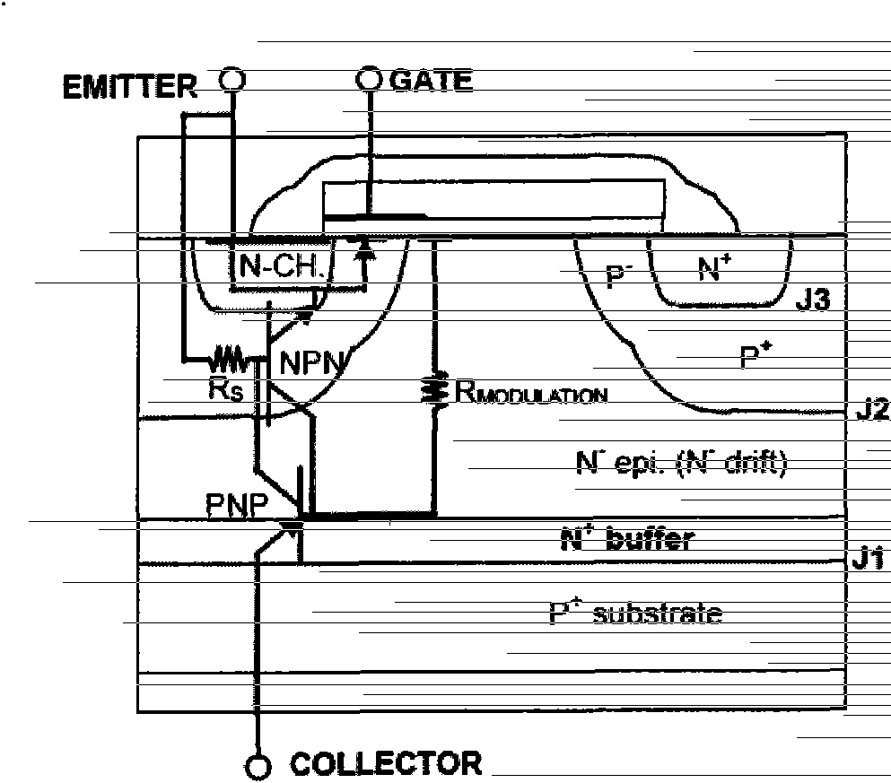
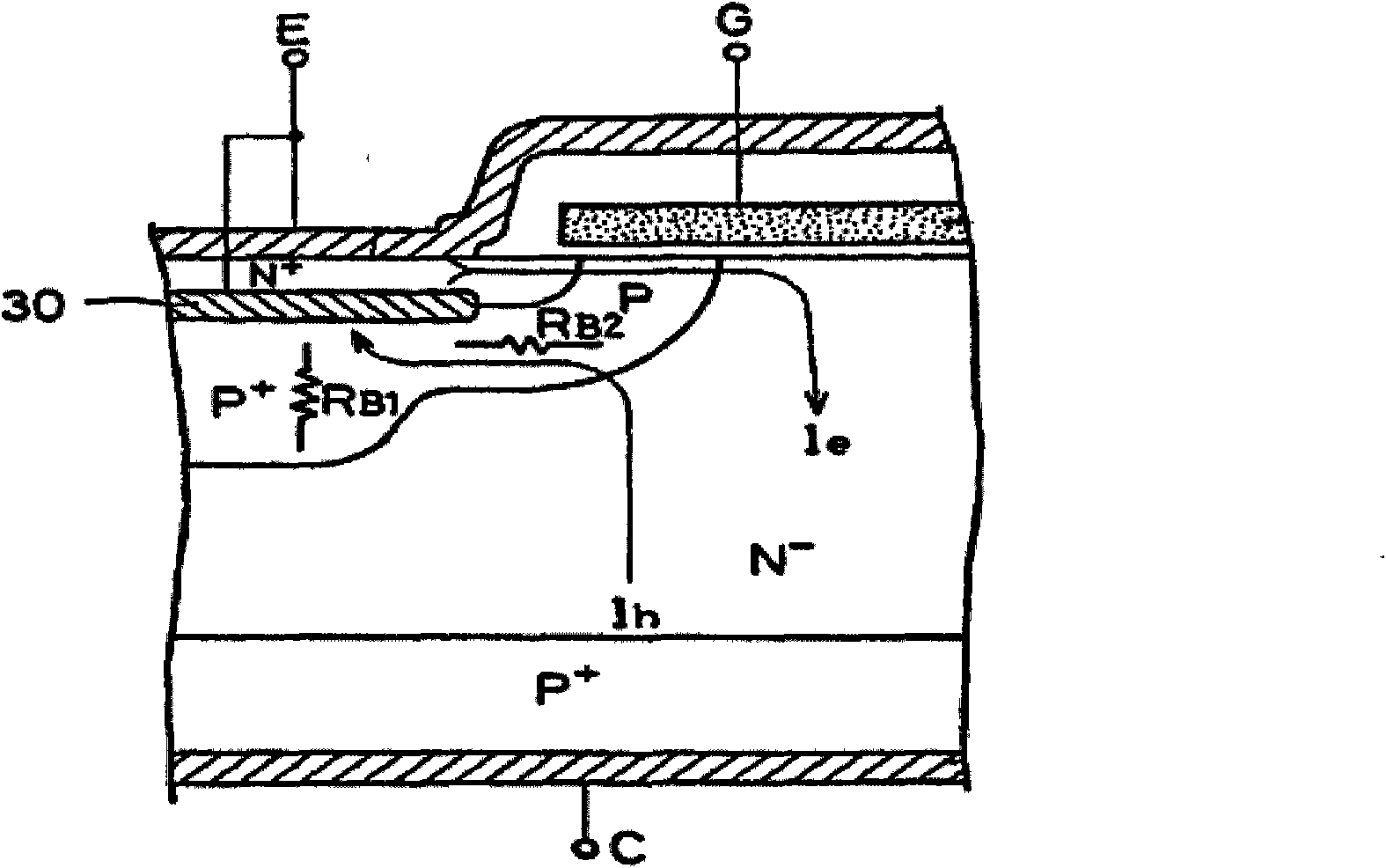
[0029] In the embodiment of the present invention, the middle part of the well region formed on the semiconductor layer is hollowed out, and an electrode contact layer flush with the surface of the semiconductor layer is filled therein, and there is a laterally diffused source region on the side of the electrode contact layer, so the size of the source region It is completely determined by the width of its lateral diffusion, that is, the lateral size of the source region of the device can be minimized.

[0030] The power semiconductor device provided by the first embodiment of the present invention...


PUM


Abstract

The invention is suitable for the technical field of semiconductors and provides a power semiconductor device and a manufacturing method thereof. The power semiconductor device comprises a semiconductor layer formed on a semiconductor substrate and a well region formed on the semiconductor layer, wherein the middle of the well region is filled with an electrode contact layer which is flush with the surface of the semiconductor layer; both sides of the electrode contact layer are provided with transversely diffused source regions; the bottom surface of the electrode contact layer is provided with a diffusion deep well; and the source regions, the deep well region and the electrode contact layer are contacted pairwise. In the invention, the middle part of the well region formed on the semiconductor layer is hollowed and filled with the electrode contact layer which is flush with the surface of the semiconductor layer, the side faces of the electrode contact layer is provided with the transversely diffused source regions and the sizes of the source regions are fully defined by transverse diffusion widths, so that the transverse sizes of the source regions of the device can be minimized, a transverse resistance which is parasitic under a P-well middle source region is reduced, a parasitic NPN tube is prevented from working in the amplification state and the latch-up of the device is restrained.

Description

technical field [0001] The invention belongs to the technical field of semiconductors, and in particular relates to a manufacturing method of a power semiconductor device. Background technique [0002] It is well known that the latch-up effect is the main factor limiting the operating current of gated transistors in power semiconductor devices. If the hole flow of the p-well channel formed under the n+ source region increases, a voltage difference exists between the p-well and the source region. When the voltage difference is higher than a certain value (about 0.7V), that is, the emitter and base of the parasitic NPN transistor are generally forward-biased, the parasitic transistor in the gate-controlled transistor starts to work, and the device latches up. Latch-up not only causes the gate of the device to lose its control function, but in severe cases, the current of the device continues to increase, causing the temperature of the chip to rise until it burns out. [000...

Claims


Application Information

Patent Timeline
Patent Type & Authority Patents(China)
IPC IPC(8): H01L29/739H01L29/06H01L21/331H01L21/768H01L21/28H01L27/082
Inventor 朱超群唐盛斌冯卫陈宇吴海平刘林
Owner BYD SEMICON CO LTD
Why Eureka
Try Eureka