
Preparation method of insulated gate bipolar transistor

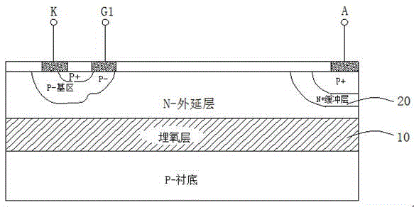
A bipolar transistor, insulated gate technology, used in semiconductor/solid-state device manufacturing, semiconductor devices, electrical components, etc., can solve the problems of complex process, slow switching speed, difficult threshold voltage control, etc., and achieve high anti-latch performance. , simplifies the structure, suppresses the effect of latch-up

Active Publication Date: 2016-06-01
广东可易亚半导体科技有限公司
View PDF4 Cites 0 Cited by
  • Summary
  • Abstract
  • Description
  • Claims
  • Application Information

AI Technical Summary

Problems solved by technology

However, the existing IGBT has disadvantages such as difficult threshold voltage control and complicated process.
In addition, although the existing IGBT has the advantages of low on-resistance, high input impedance and simple driving circuit, it also has disadvantages such as relatively slow switching speed.

Method used


Image

  • Preparation method of insulated gate bipolar transistor
  • Preparation method of insulated gate bipolar transistor
  • Preparation method of insulated gate bipolar transistor

Examples


Embodiment Construction

[0021] The specific implementation manners of the present invention will be described in detail below in conjunction with the accompanying drawings.

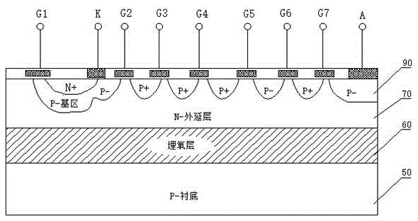
[0022] A method for preparing an insulated gate bipolar transistor, comprising the steps of:

[0023] S1. Forming a p-type semiconductor substrate 50 having a doping concentration of impurities of a predetermined conductivity type;

[0024] S2. After growing the buried oxide layer 60 on the p-type substrate, forming an n-type epitaxial layer 70 on the buried oxide layer 60;

[0025] S3. Implanting p-type impurity ions on one side of the n-type epitaxial layer 70 to form a p- / p+ base region with a predetermined depth; implanting p-type impurity ions on the other side of the n-type epitaxial layer to form a base region with a predetermined depth. A p+ ring 90 of a predetermined depth; implanting n-type impurity ions into the p- / p+ base region to form an n+ region of a predetermined depth;

[0026] S4, forming a first gate and a ...


PUM


Abstract

The invention discloses a preparation method of an insulated gate bipolar transistor. The method comprises the following steps: forming a p-type semiconductor substrate; growing a buried oxide layer on the p-type substrate and forming an n-type epitaxial layer on the buried oxide layer; injecting p-type impurity ions into one side of the n-type epitaxial layer and forming a p- / p+ base region with a predetermined depth; injecting the p-type impurity ions into the other side of the n-type epitaxial layer and forming a p+ ring with the predetermined depth; injecting n-type impurity ions into the p- / p+ base region and forming an n+ region with the predetermined depth; forming a first gate and a cathode on the p- / p+ base region and forming an anode on the p+ ring and forming a second gate between the cathode and the anode. The preparation method of the insulated gate bipolar transistor disclosed by the invention aims at providing the preparation method of the insulated gate bipolar transistor, which has high latch resistance and can quickly finish switching.

Description

technical field [0001] The invention relates to the technical field of processing technology of semiconductor components, in particular to a preparation method of an insulated gate bipolar transistor. Background technique [0002] Insulated gate bipolar transistor (InsulatedGateBipolarTransistor: IGBT) is a very suitable device for smart (smart) power supply IC due to its small forward voltage drop and large input impedance; ) (A), a parasitic thyristor composed of n-type epitaxial layer (or drift layer), p base region and n+ cathode (K). When the IGBT works normally, the parasitic thyristor does not work, but when the current exceeds a certain value, the parasitic thyristor turns on, which is the latch characteristic. When the latch-up effect occurs, the IGBT will lose the control capability of the MOS gate, and at the same time, the latch-up effect will limit the current control capability of the IGBT and determine the safe working area; [0003] In order to make the hol...

Claims


Application Information

Patent Timeline
IPC IPC(8): H01L21/331H01L21/28H01L29/739H01L29/06
CPCH01L21/28H01L29/06H01L29/66325H01L29/7393
Inventor 赵喜高
Owner 广东可易亚半导体科技有限公司
Learn More