Display panel pixel

A display panel and pixel technology, applied in the pixel field, can solve the problem that the characteristics of the switching transistor drive transistor do not meet the design requirements, and achieve the effect of improving the characteristics

Active Publication Date: 2014-07-02
AU OPTRONICS CORP
View PDF9 Cites 0 Cited by
  • Summary
  • Abstract
  • Description
  • Claims
  • Application Information

AI Technical Summary

Problems solved by technology

[0003] However, in the prior art, both the switching transistor and the driving transistor of the OLED pixel are manufactured in the same manufacturing process, that is to say, the sub-threshold swings of the switching transistor and the driving transistor of the existing OLED pixel are the same , the above situation may cause the characteristics of the switching transistor and / or driving transistor to not meet the design requirements

Method used


Image

  • Display panel pixel
  • Display panel pixel
  • Display panel pixel

Examples


Embodiment Construction

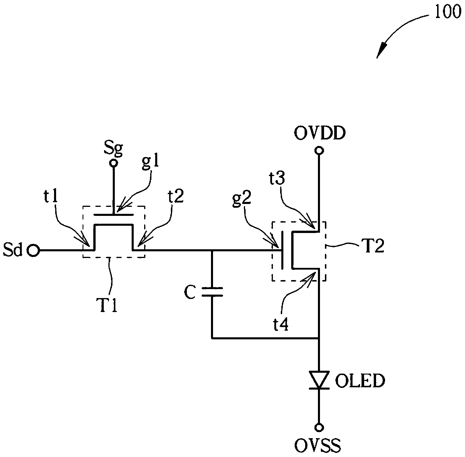
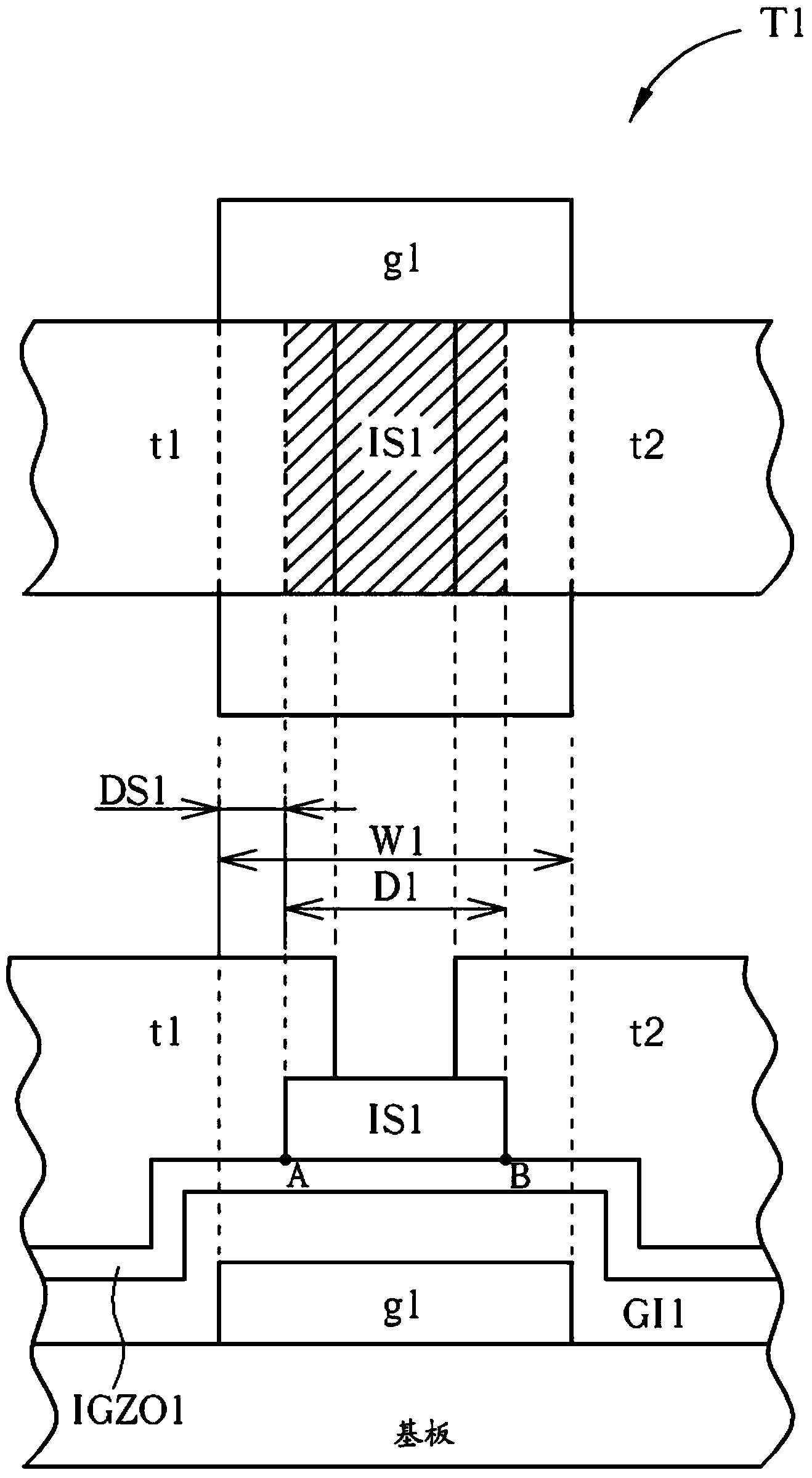
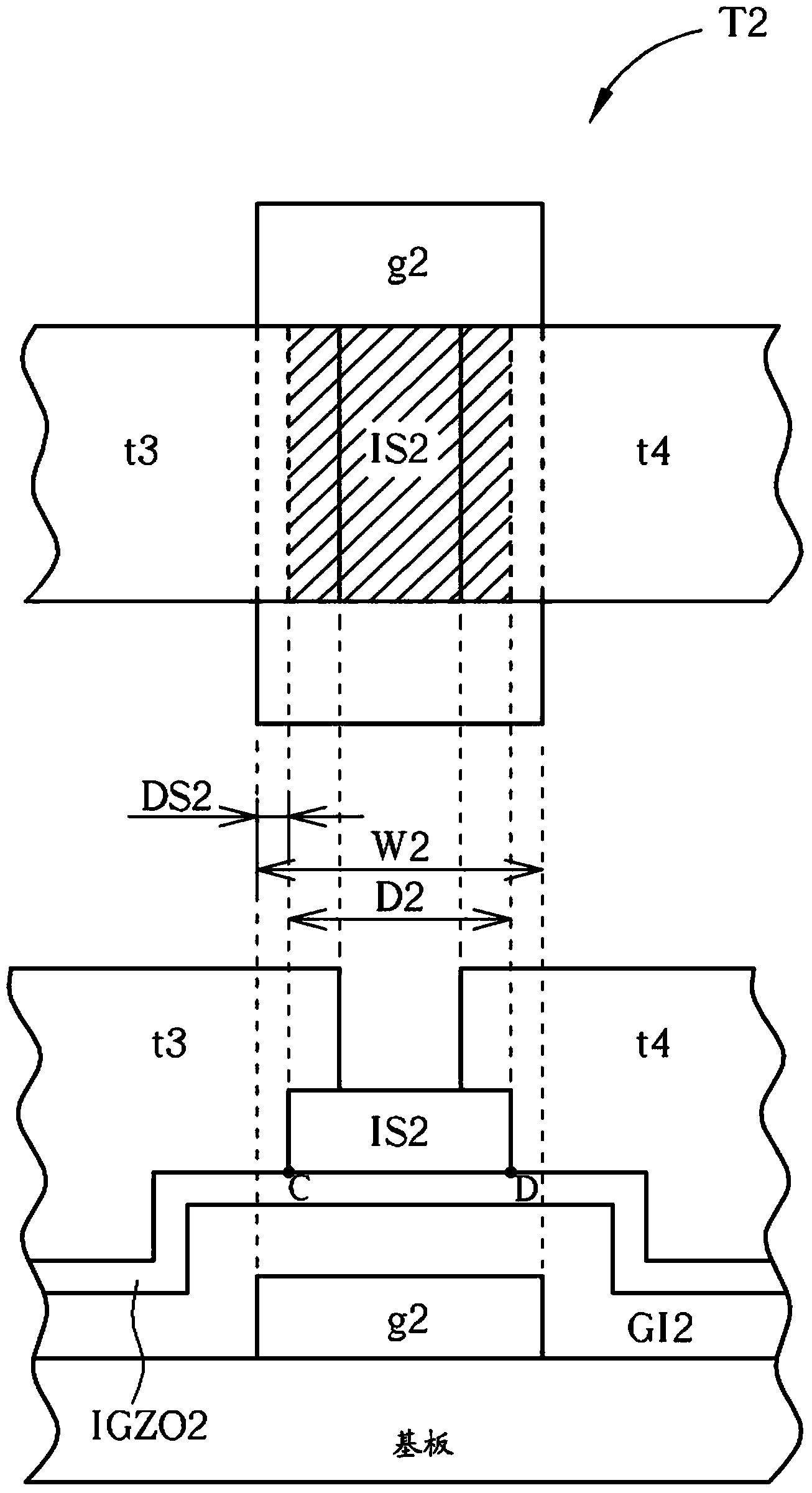
[0039] Please refer to figure 1 . figure 1 It is a schematic circuit diagram of a pixel of the display panel of the present invention. Such as figure 1 As shown, the pixel 100 of the display panel of the present invention includes a first transistor T1, a light emitting unit OLED, a capacitor C, and a second transistor T2. The first transistor T1 is used as a switch transistor, and the second transistor T2 is used as a driving transistor. The first transistor T1 has a first electrode t1, a second electrode t2 and a first gate electrode g1. The first electrode t1 is used for receiving the data signal Sd. The first gate electrode g1 is used for receiving the scan signal Sg to control the conduction or cut-off between the first electrode t1 and the second electrode t2 according to the scan signal Sg. When the first electrode t1 and the second electrode t2 are conducted, the data signal Sd will be written into the capacitor C. The light emitting unit OLED has a first termina...


PUM


Abstract

The invention discloses a display panel pixel comprising a first transistor, a first electrode, a second electrode and a first gate electrode; the first electrode is used to receive a data signal; the first gate electrode is used for receiving a scan signal; the light emitting unit is provided with a first end and a second end; the second end is coupled to the first voltage source; and a second transistor is provided with a third electrode, a fourth electrode and a second gate electrode; the second gate electrode is coupled to the second electrode; the fourth electrode is coupled to the first end of the light emitting element; the distance difference between the first gate electrode parallel to the first and second electrode wire width and the first electrode and the second electrode is greater than that of the second gate electrode in parallel between the third and fourth line of the width of the electrode and the third electrode and the fourth electrode.

Description

technical field [0001] The present invention relates to a pixel of a display panel, in particular to a transistor structure in a pixel of a display panel. Background technique [0002] An organic light emitting diode display is a display device that uses organic light emitting diode pixels to emit light to display images. The brightness of an OLED is proportional to the magnitude of the current flowing through the OLED. Generally, an OLED pixel includes two transistors, one is a switching transistor and the other is a driving transistor. The switch transistor is used to control the writing of the data signal according to the scanning signal, and the driving transistor is used to control the magnitude of the driving current flowing through the OLED according to the voltage of the written data signal. [0003] However, in the prior art, both the switching transistor and the driving transistor of the OLED pixel are fabricated in the same manufacturing process, that is to say,...

Claims


Application Information

Patent Timeline
Patent Type & Authority Applications(China)
IPC IPC(8): G09G3/32G09G3/3266G09G3/3275
Inventor 谢毅翰
Owner AU OPTRONICS CORP
Why Eureka
Try Eureka