Pixel unit, pixel unit manufacturing method, TFT (thin film transistor) array substrate and display device

A technology of pixel unit and manufacturing method, applied in the field of pixel unit and its manufacture, TFT array substrate, and display device, can solve the problem of low light transmittance above the pixel electrode, and achieve the effect of avoiding dark areas

Active Publication Date: 2014-07-09
XIAMEN TIANMA MICRO ELECTRONICS +1
View PDF4 Cites 6 Cited by
  • Summary
  • Abstract
  • Description
  • Claims
  • Application Information

AI Technical Summary

Problems solved by technology

[0006] In view of this, an embodiment of the present invention provides a pixel unit and its manufacturing method, a TFT array substrate, and a display device to solve the problem of low light transmittance above the pixel electrode existing in the prior art

Method used


Image

  • Pixel unit, pixel unit manufacturing method, TFT (thin film transistor) array substrate and display device
  • Pixel unit, pixel unit manufacturing method, TFT (thin film transistor) array substrate and display device
  • Pixel unit, pixel unit manufacturing method, TFT (thin film transistor) array substrate and display device

Examples


Embodiment 1

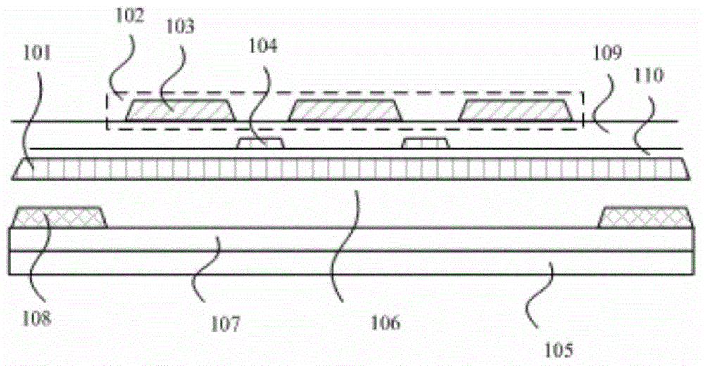
[0032] Such as figure 2 As shown, it is a sectional view of a pixel unit provided in Embodiment 1 of the present invention, which mainly includes the following structural units:

[0033] The pixel electrode 101.

[0034] Generally, the pixel electrode 101 is a planar electrode located on the fourth insulating layer 106 of the substrate 105 , and a gate insulating layer 107 and a data line 108 are also disposed between the fourth insulating layer 106 and the substrate 105 .

[0035] The common electrode 102 is located above the pixel electrode 101 and insulated from the pixel electrode 101 , and the common electrode includes at least two branch electrodes 103 .

[0036] Preferably, the thickness of the common electrode branch electrode 103 can generally be set to 40nm˜50nm.

[0037] Wherein, the material of the pixel electrode 101 and the common electrode 102 can be transparent conductive material.

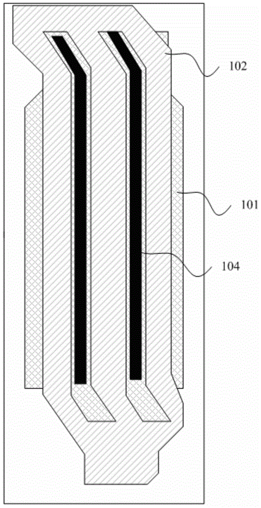
[0038] A plurality of shielding electrodes 104, located between the pixel ...

Embodiment 2

[0054] Such as Figure 5 As shown, the cross-sectional view of the pixel unit provided by Embodiment 2 of the present invention mainly includes the following structural units:

[0055] common electrode 201 .

[0056] In this case, the common electrode 201 is a planar electrode located on the fourth insulating layer 206 of the substrate 205, and a gate insulating layer 207 and a data line 208 are also arranged between the fourth insulating layer 206 and the substrate 205 .

[0057] The pixel electrode 202 is located above the common electrode and insulated from the common electrode, and the pixel electrode includes at least two branch electrodes 203 .

[0058] Preferably, the thickness of the pixel electrode branch electrode 203 can generally be set to 40 nm˜50 nm, and the width of the pixel electrode branch electrode is 3.5 μm˜5 μm.

[0059] A plurality of shielding electrodes 204 are located directly above each branch electrode of the pixel electrode, and each shielding el...

example 1

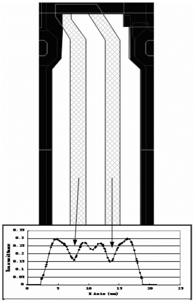
[0067] As shown in FIG. 7( a ), it is the first group of simulation diagrams of the second embodiment of the present invention.

[0068] Among them, the common electrode is a planar electrode, and the pixel electrode has at least two strip-shaped branch electrodes, which are arranged as shown in the left figure, with the common electrode at the bottom and the pixel electrode at the top, and the width of the pixel electrode branch electrodes is 3.5 μm, and the distance between branch electrodes of each pixel electrode is 3.4 μm. When the pixel unit formed with the above structure is tested, the transmittance simulation diagram in the left figure is obtained. According to the analysis, it can be known that the light transmittance is relatively low near the position above the branch electrode corresponding to each pixel electrode. After further analysis, it can be determined that the branch electrodes of the pixel electrodes generate an electric field perpendicular to the substra...


PUM

PropertyMeasurementUnit
thicknessaaaaaaaaaa
thicknessaaaaaaaaaa
widthaaaaaaaaaa

Abstract

The invention discloses a pixel unit, a pixel unit manufacturing method, a TFT (thin film transistor) array substrate and a display device. The pixel unit is mainly characterized in that when a pixel electrode is positioned under a common electrode, shielding electrodes are arranged between the common electrode and the pixel electrode and insulated from the pixel electrode and the common electrode, and each shielding electrode is positioned between two adjacent branch electrodes of the common electrode. Therefore, the shielding electrodes can offset part of a perpendicular electric field generated by the pixel electrode, so that light transmittance cannot be affected by a liquid crystal alignment mode, and a dark zone generated right above the pixel electrode is avoided.

Description

technical field [0001] The invention relates to the field of display technology, in particular to a pixel unit, a manufacturing method thereof, a TFT array substrate, and a display device. Background technique [0002] In the prior art, because the liquid crystal display device of the FFS display mode is easy to manufacture and can achieve a wide viewing angle, this display mode becomes the most attractive way to improve viewing angle characteristics and realize large-area display. [0003] However, in the liquid crystal display device in the FFS display mode, the pixel electrode and the common electrode are located on the side of the lower substrate (TFT array substrate) and are in different film layers, so there will be an edge between the pixel electrode and the adjacent common electrode. The electric field causes the center of the pixel electrode to be approximately a vertical electric field (that is, the lines of force are arranged upwards or downwards), which in turn m...

Claims


Application Information

Patent Timeline
Patent Type & Authority Applications(China)
IPC IPC(8): G02F1/1343G02F1/1333
Inventor 宋琼沈柏平张沼栋
Owner XIAMEN TIANMA MICRO ELECTRONICS
Why Eureka
Try Eureka