


Quick Research
Generate reliable direction feasibility study reports for your R&D in just a few steps.

Technical Q&A
Discover and master advanced knowledge NOW. Basics, ideas, possibilities, all at once.

Find Solutions
As an expert in R&D theories, this can generate solutions to your technical problems instantly.

Evaluate Feasibility
Analyze your overall solution with one click, know your potential R&D risks in advance.

Monitor Landscape
Get weekly tech updates, stay abreast of the latest tech innovations and key insights.
TFT array substrate, display panel and display device
A technology for array substrates and pixel units, applied in the field of display panels and display devices, and TFT array substrates, can solve the problem of different sizes of pixel units 11 and 12, and achieve the effect of improving transmittance
- Summary
- Abstract
- Description
- Claims
- Application Information
AI Technical Summary
Problems solved by technology
Method used
Image

Examples
Embodiment 1
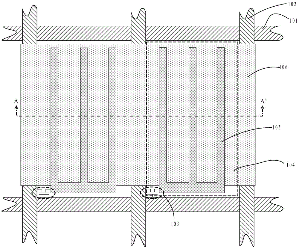
[0034] The top view structure schematic diagram of the pixel in the TFT array substrate provided by Embodiment 1 of the present invention is as follows Figure 7 shown ( Figure 7 only shows the local structure of two adjacent pixel units), Figure 8 for Figure 7 Schematic diagram of the cross-sectional structure along the DD’, Figure 9 for Figure 7 Schematic diagram of the cross-sectional structure along EE'. From Figure 7 , 8 , 9, it can be seen that the TFT array substrate provided in Embodiment 1 includes:
[0035] a plurality of scan lines 201 (two adjacent scan lines 2011 and 2012 are shown in the figure);
[0036] A plurality of data lines 202 (three adjacent data lines 2021 , 2022 and 2023 are shown in the figure) that insulate and intersect with the plurality of scan lines 201 ;
[0037] A pixel unit located in a pixel area surrounded by adjacent scan lines and adjacent data lines (two adjacent pixel units PIX1 and PIX2 are shown in the figure).
[0038] ...
Embodiment 2
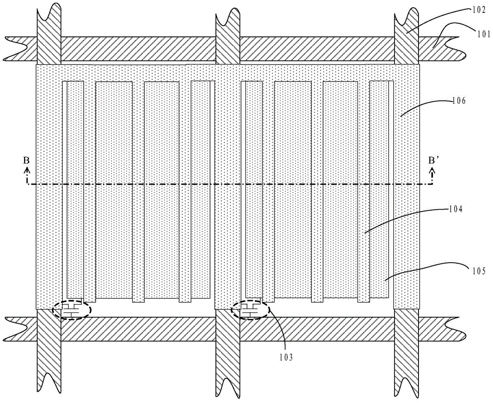
[0052] The top view structure schematic diagram of the pixel in the TFT array substrate provided by the second embodiment of the present invention is as follows Figure 11 as shown ( Figure 11 only shows the local structure of two adjacent pixel units), Figure 12 for Figure 11 Schematic diagram of the cross-sectional structure of the middle edge FF', Figure 13 for Figure 11 Schematic diagram of the cross-sectional structure along GG' in the middle. From Figure 11 , 12 13, it can be seen that the second embodiment is similar to the first embodiment, the similarities between the two will not be repeated, and the differences between the two will be emphasized. compared to Figure 7 , 8 , Embodiment 1 shown in 9, 10, Figure 11 , 12 The difference between the second embodiment shown in 13 and 13 is that no shielding electrodes are provided above the data lines 2021 , 2022 , 2023 , that is, they are not covered by the shielding electrodes. Therefore, the common ele...
Embodiment 3
[0059] The top view structure schematic diagram of the pixel in the TFT array substrate provided by the third embodiment of the present invention is as follows Figure 14 as shown ( Figure 14 only shows the local structure of two adjacent pixel units), Figure 15 for Figure 14 Schematic diagram of the cross-sectional structure along HH', Figure 16 for Figure 7 Schematic diagram of the cross-sectional structure along II'. From Figure 14 , 15 , 16, it can be seen that the third embodiment has similarities and differences with the first and second embodiments. The main difference is that in the third embodiment, the pixel electrode is comb-shaped and includes a plurality of strip electrodes; the common electrode is sheet-shaped; the pixel electrode is located above the common electrode and is insulated from the common electrode. The TFT array substrate of the third embodiment further includes a shielding electrode, which is formed by extending the sheet-shaped common ...
PUM
 Abstract
Description
Claims
Application Information
 - R&D Engineer
- R&D Manager
- IP Professional
- Industry Leading Data Capabilities
- Powerful AI technology
- Patent DNA Extraction
Browse by: Latest US Patents, China's latest patents, Technical Efficacy Thesaurus, Application Domain, Technology Topic, Popular Technical Reports.
© 2024 PatSnap. All rights reserved.Legal|Privacy policy|Modern Slavery Act Transparency Statement|Sitemap|About US| Contact US: help@patsnap.com