Array substrate, display panel and display device

A technology for array substrates and display areas, applied to semiconductor/solid-state device parts, instruments, semiconductor devices, etc., to achieve the effect of reducing width and realizing narrow frame design

Active Publication Date: 2014-07-23
SHANGHAI TIANMA MICRO ELECTRONICS CO LTD +1
View PDF3 Cites 52 Cited by
  • Summary
  • Abstract
  • Description
  • Claims
  • Application Information

AI Technical Summary

Problems solved by technology

[0005] The display panels of the prior art still have the problem of further realizing narrower borders

Method used


Image

  • Array substrate, display panel and display device
  • Array substrate, display panel and display device
  • Array substrate, display panel and display device

Examples


Embodiment Construction
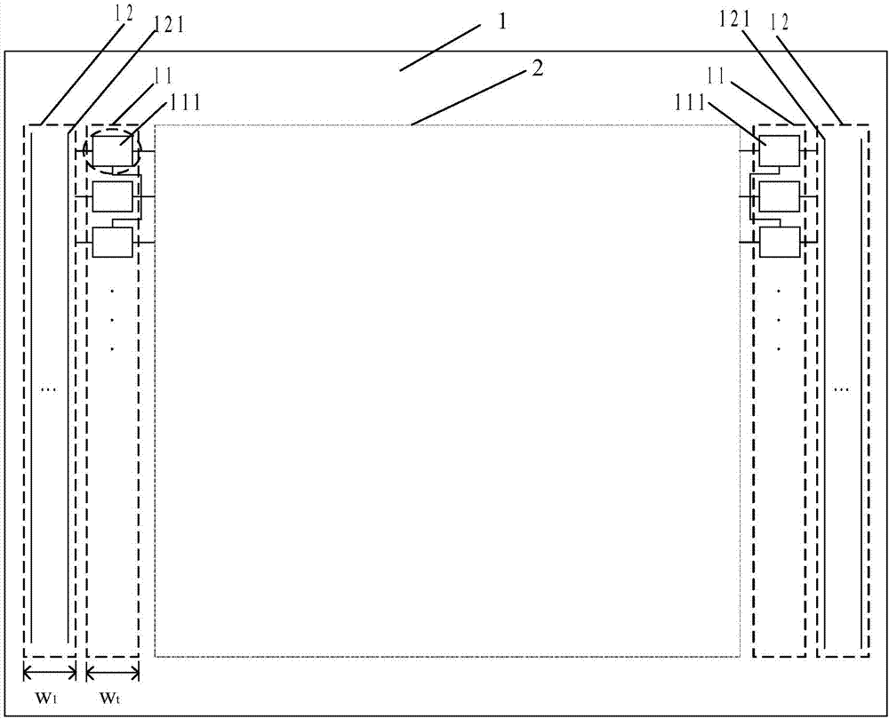
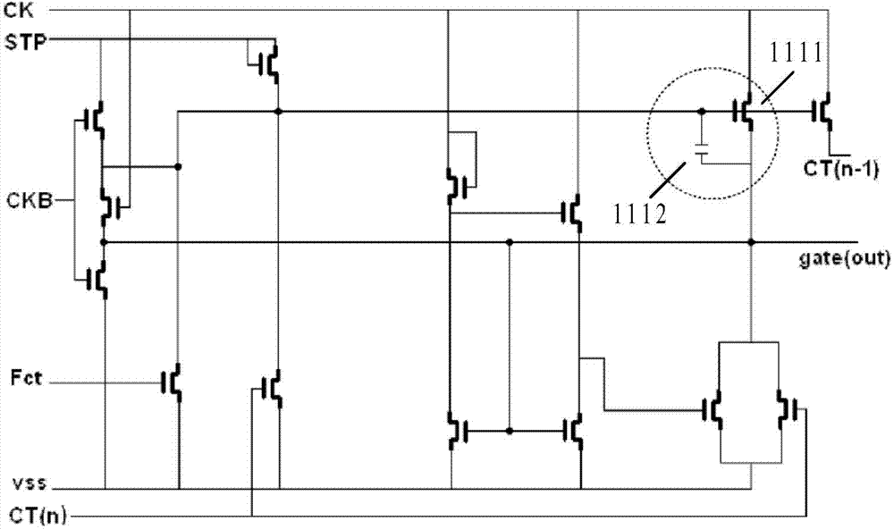
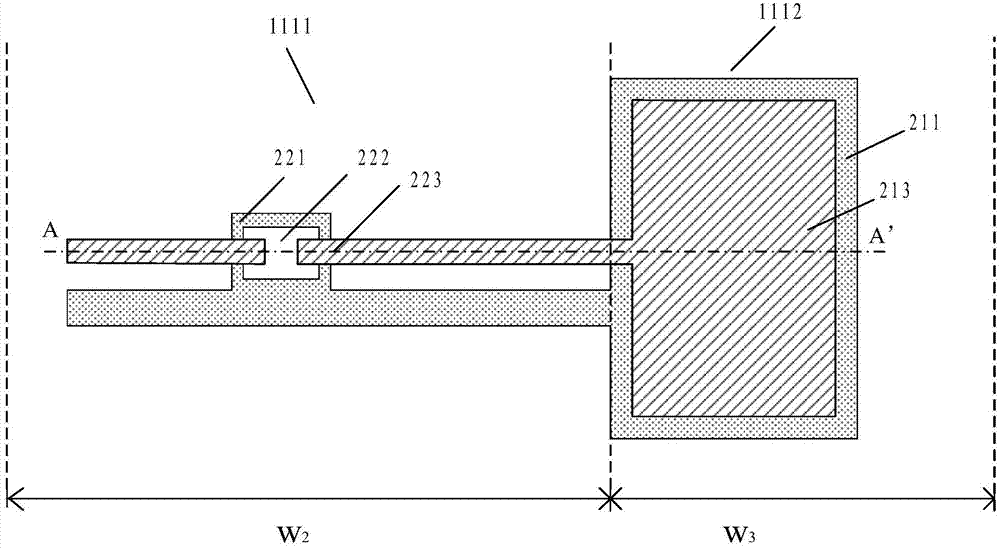
[0024] The core idea of ​​the present invention is that by disposing the capacitor above or below the signal line, the capacitor does not occupy the width of the frame alone, thereby further reducing the width of the frame of the display device and realizing a narrow frame design.

[0025] Embodiment 1 of the present invention provides an array substrate, such as Figure 4 As shown in FIG. 1 , it is a schematic top view structural diagram of the array substrate provided by the embodiment of the present invention. The array substrate provided by the embodiment of the present invention includes: a display area 42 and a non-display area 41, wherein the display area 42 is provided with a plurality of gate lines 421, and a plurality of data lines 422 insulated and intersected with the plurality of gate lines are arranged in opposite A pixel unit adjacent to the area surrounded by the data line and the adjacent gate line includes a TFT 423 as a pixel switch and a pixel electrode 424...


PUM


Abstract

The invention discloses an array substrate, a display panel and a display device. The array substrate comprises a display area and a non-display area. The non-display area is provided with a grid drive circuit and a signal line located outside the grid drive circuit. The grid drive circuit comprises at least one TFT and at least one capacitor. The capacitor comprises a first electrode plate and a second electrode plate, and is located above or below the signal line. Due to the fact that the capacitor part in the grid drive circuit does not need to be arranged additionally, the size of the grid drive circuit can be reduced, the width of the frame of the display device is reduced, and the narrow frame design is achieved.

Description

technical field [0001] The present invention relates to the display field, in particular to an array substrate, a display panel and a display device including the array substrate. Background technique [0002] With the development of display technology, the design of display devices tends to be narrower, with larger screens and narrower frames. The narrow frame enlarges the screen without increasing the size of the device, thereby improving the display effect of the display device. [0003] In the prior art for realizing narrow borders, integrating the gate driving circuit on the display panel is one of the most important solutions. Directly integrating the gate driver circuit in the display panel, replacing the original gate driver IC (Gatedriver IC), can not only reduce product cost in terms of material cost and manufacturing process, make the display screen lighter, but also improve product quality. Reliability, beautiful design with narrow frame. The structure of the ...

Claims


Application Information

Patent Timeline
Patent Type & Authority Applications(China)
IPC IPC(8): G02F1/1362G02F1/1368H01L27/12
CPCH01L23/5223H01L2924/0002H01L27/1255H01L2924/00H01L23/5226H01L27/124H01L27/1248
Inventor 王超曹兆铿
Owner SHANGHAI TIANMA MICRO ELECTRONICS CO LTD
Why Eureka
Try Eureka