Printed circuit board stack

A printed circuit substrate and printed circuit technology, applied in the directions of printed circuit, printed circuit, stacking and separating printed circuit boards, etc., can solve the problem of not being able to fully guarantee the connection stability, etc., to improve the connection stability and achieve miniaturization. , the effect of using space

Inactive Publication Date: 2014-07-23
SUMITOMO WIRING SYST LTD
View PDF5 Cites 1 Cited by
  • Summary
  • Abstract
  • Description
  • Claims
  • Application Information

AI Technical Summary

Problems solved by technology

Therefore, there is a concern that solder cracks are likely to occur at the soldered portion of the connection terminal between the boards, and it cannot be said that the connection stability between the two boards is sufficiently ensured.

Method used


Image

  • Printed circuit board stack
  • Printed circuit board stack
  • Printed circuit board stack

Examples


Embodiment Construction

[0026] Hereinafter, embodiments of the present invention will be described with reference to the drawings.

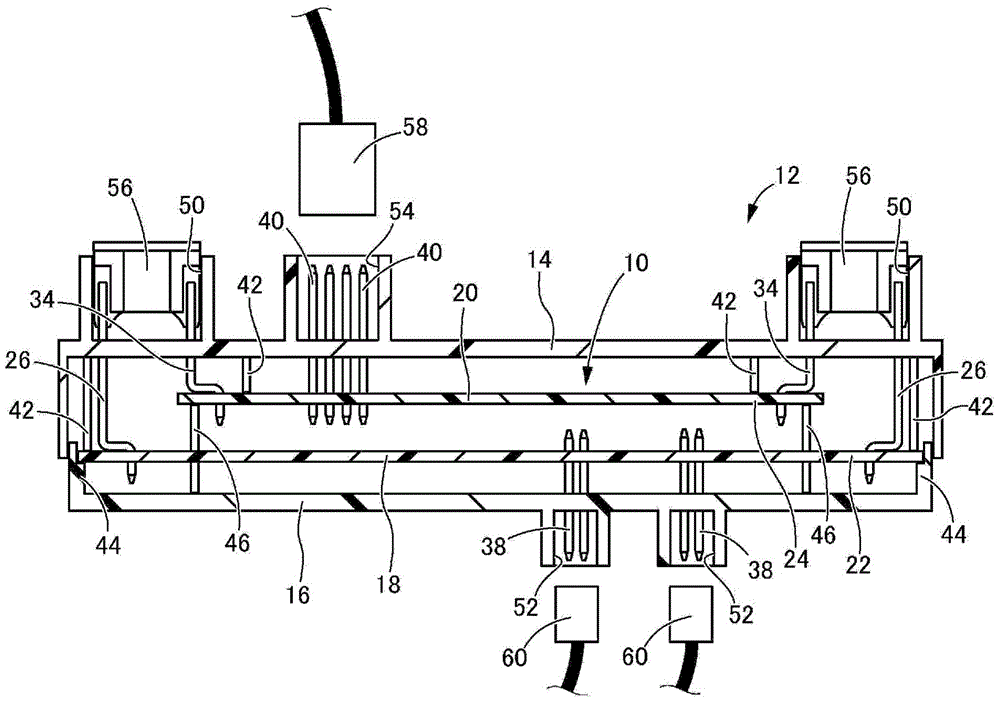
[0027] First, in figure 1 The electrical junction box 12 provided with the printed circuit board laminated body 10 which is 1st Embodiment of this invention is shown. The electrical junction box 12 has a structure in which the printed circuit board laminate 10 is accommodated between an upper case 14 and a lower case 16 formed of synthetic resin. In addition, in the following description, the upper side refers to the side that is the upper case 14 side. figure 1 The upper and lower refer to the side of the lower housing 16 as the figure 1 in the bottom.

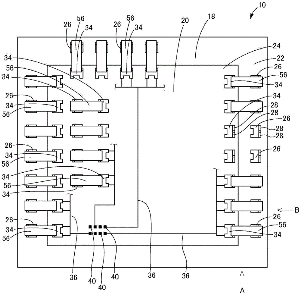
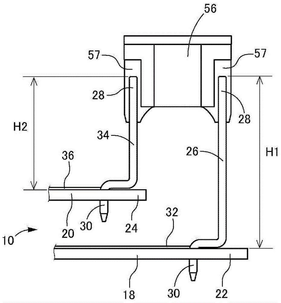
[0028] figure 2 The upper surface of the printed circuit board laminate 10 is shown, and in image 3 and Figure 4 The main part of the printed circuit board laminated body 10 is shown. In addition, in Figure 2 ~ Figure 4 In , for easy understanding, a fuse 56 to be described later is shown together. The pri...


PUM


Abstract

Provided is a printed circuit board stack having a new structure that can connect between printed wirings of printed circuit boards that are arranged so as to face each other across a gap, with an improved operability and connection stability. With respect to a first printed circuit board (18) and a second printed circuit board (20) that are arranged so as to face each other across a gap, a first fork terminal (26) that is soldered to a printed wiring (32) is vertically provided on the first printed circuit board (18), whereas a second fork terminal (34) that is soldered to a printed wiring (36) is vertically provided on the second printed circuit board (20). The printed wiring (32) of the first printed circuit board (18) and the printed wiring (36) of the second printed circuit board (20) are electrically connected to each other via a conductive member (56) that is provided with a pair of connection portions (57) that each are pressure-contacted between pressure contact blades (28) of each of the first fork terminal (26) and the second fork terminal (34).

Description

technical field [0001] The present invention relates to a printed circuit board laminate in which two printed circuit boards facing each other with a gap therebetween are electrically connected via a conduction member connected to each printed circuit wiring. Background technique [0002] Conventionally, as an electrical junction box mounted on an automobile, an electrical junction box that accommodates a printed circuit board therein to configure an internal circuit is known. In particular, in recent years, along with the increase of in-vehicle electrical equipment, etc., as described in Japanese Patent Application Laid-Open No. 7-297562 (Patent Document 1), a printed circuit board including two printed circuit boards facing each other with a gap between them is disclosed. Electrical connection box for circuit board laminates. [0003] However, in such a printed circuit board laminate, in order to connect the respective printed circuit wirings of the two printed circuit bo...

Claims


Application Information

Patent Timeline
Patent Type & Authority Applications(China)
IPC IPC(8): H01R12/71
CPCH01R12/523H05K1/144H05K7/026H05K2201/042H05K2201/10181H05K2201/10295H05K2201/10303
Inventor 石文杰
Owner SUMITOMO WIRING SYST LTD
Why Eureka
Try Eureka