Liquid crystal display device and method for manufacturing the same

a liquid crystal display and display device technology, applied in the direction of microlithography exposure apparatus, identification means, instruments, etc., can solve the problems of high power dissipation, large volume, heavy weight, etc., and achieve the effect of greatly reducing the step between the pads, preventing the electrical short between the pads of the lcd device, and greatly reducing the fp

Inactive Publication Date: 2006-01-10
TCL CHINA STAR OPTOELECTRONICS TECH CO LTD
View PDF11 Cites 27 Cited by
  • Summary
  • Abstract
  • Description
  • Claims
  • Application Information

AI Technical Summary

Benefits of technology

[0042]According to the present invention, it can be minimized that the difference in height between one portion of the organic insulation layer in the pad region and the other portion of the organic insulation layer adjacent to the pad region by exposing and developing single organic insulation layer or double organic insulation layers. Therefore, the connection failure between the pads of the LCD device and the COG, the COF, the FPC can be greatly decreased when the COG, the COF, the FPC is compressed to the pads of the LCD device. Also, the electrical short between the pads of the LCD device can be prevented since the organic insulation layer remains between the pads while the step between the pads is greatly decreased. Furthermore, the step in the pad region can be minimized without performing another process for reducing the step since it is reduced that the height difference between the height difference between one portion of the organic insulation layer in the pad region and the other portion of the organic insulation layer adjacent to the pad region when the organic insulation layer is exposed and developed so as to from the contact hole and the reflection electrode.

Problems solved by technology

The CRT, however, has some disadvantages such as a heavy weight, a large volume and high power dissipation.
In the conventional method for manufacturing the LCD device, however, since the organic insulation layer or a layer having thick thickness is formed on the TFT as a protection layer, the connection failure between an external device and the LCD device may occur due to the step between the pad region having the metal formed thereunder and the peripheral region when the external device such as the COG, the COF or the FPC is connected to the pad region of the LCD device.
Thus, the LCD device module may not operate or operate improperly due to the connection failure.
In particular, the connection failure between the COG and the pad may be increased since the COG is connected to the pad by using the conductive ball with a diameter of about 5 μm during the conventional compression process.
Also, electrical shorts between adjacent pads become more likely may be increased when the organic insulation layer formed on the pads and the peripheral region is removed because the organic insulation layer prevents the electrical short between the adjacent pads among a plurality of pads, whereby reducing the reliability of the product.

Method used


Image

  • Liquid crystal display device and method for manufacturing the same
  • Liquid crystal display device and method for manufacturing the same
  • Liquid crystal display device and method for manufacturing the same

Examples


embodiment 1

[0051]FIG. 3 is a plane view illustrating a method for manufacturing an LCD device according to a first embodiment of the present invention and FIGS. 4A, 4B and 4C are cross-sectional views taken along line A-A′ in FIG. 3 for showing manufacturing steps of the LCD device according to the first embodiment of the present invention.

[0052]In a reflection type LCD device or a semi-transmissive type LCD device, in order to form a prominence and depression portions on a reflection electrode, the reflection electrode is coated on an organic insulation layer having a rugged surface to have a rugged shape after the organic insulation layer is exposed and developed to have the prominence and the depression portions on the surface of the organic insulation layer. A full exposure process for double organic insulation layers, a partial exposure process for a single organic insulation layer or a silt exposure process for a single organic insulation layer can be presented as the process for forming...

embodiment 2

[0071]In the first embodiment of the present invention, the second organic insulation layer is formed in the second region after the first organic insulation layer is removed through the full exposing process. However, the second organic insulation layer may be formed after an insulation layer pattern for forming the rugged structure on the first region corresponding to the active region. Thus, the insulation layer pattern for forming the rugged structure is previously formed on the organic insulation layer in the first region according a second embodiment of the present invention.

[0072]FIGS. 5A, 5B, 5C and 5D are schematic cross-sectional views illustrating a method for manufacturing an LCD device according the second embodiment of the present invention.

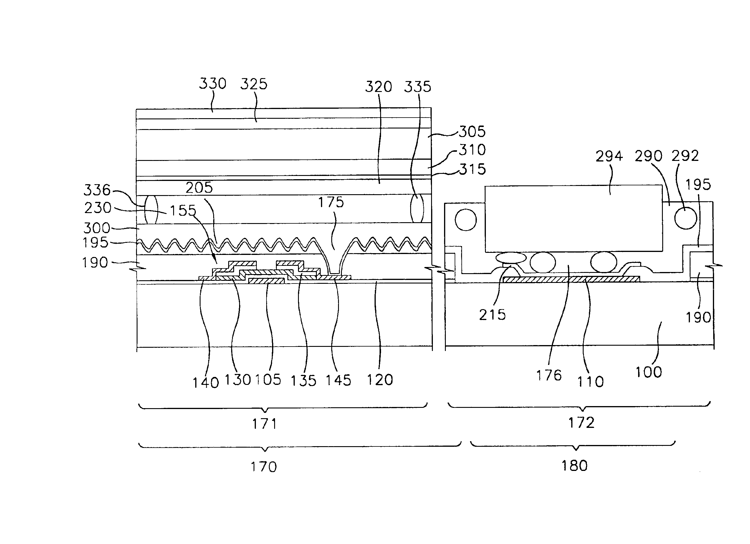
[0073]Referring to FIG. 5A, a first organic insulation layer 190 is formed on a first region 170 of a first substrate 100 where a TFT 155 is formed according the processes shown in FIGS. 4A, 4B and 4C. Then, a first insulation layer...

embodiment 3

[0085]FIGS. 6A, 6B, 6C and 6D are cross-sectional views for illustrating a process for forming an organic insulation layer according to a third embodiment of the present invention. While the double organic insulation layers are formed in accordance with the first and the second embodiments, a single organic insulation layer is formed to reduce a step in a pad region according to the present embodiment.

[0086]A TFT 155 is formed on a first substrate 100 according to the processes described in FIGS. 4A, 4B and 4C. Referring to FIG. 6A, an organic resist is coated on a first region 170 and a second region 180 of the first substrate 100 having the TFT 155 thereon by the spin coating method to form an organic insulation layer 165 having a thickness of about 2.4 to about 4.0 μm.

[0087]Subsequently, after a first mask 185 is positioned over the organic insulation layer 165 for forming a contact hole 175 and an opening 176 respectively exposing a drain electrode 145 of the TFT 155 and a pad 1...


PUM

PropertyMeasurementUnit
thicknessaaaaaaaaaa
thicknessaaaaaaaaaa
diameteraaaaaaaaaa

Abstract

An LCD device having improved connection stability concerning a COG, a COF or an FPC and a method for manufacturing the LCD device are disclosed. A pixel including a TFT as a switching device is formed at a central portion corresponding to an active region of a substrate. A gate and a data input pads are formed at a peripheral portion corresponding to a pad region of a substrate. An organic insulation layer is formed on the whole surface of the substrate having the TFT the pads thereon. A rugged structure is formed on the organic insulation layer for forming a rugged reflection electrode by exposing and developing the organic insulation layer. An organic insulation layer is formed to reduce a step between the pads and the portion adjacent to the pads. A single organic insulation layer or double organic insulation layers can be formed. A connection failure between the pads and the COG, the COF or the FPC can be greatly reduced since the height difference of the organic insulation layer between the pads the portion adjacent to the pads can be minimized through the exposing and the developing processes. Also, an electrical short between the pads can be prevented because the organic insulation layer is interposed between the pads.

Description

BACKGROUND OF THE INVENTION[0001]1. Field of the Invention[0002]The present invention relates to a method for a liquid crystal display device (LCD) and a method for manufacturing the same, more particularly to an LCD device having enhanced connection stability between a driving circuit of the LCD device and chip on glass (COG), a chip on film (COF) or a flexible printed circuit film (FPC) and a method for manufacturing the same.[0003]2. Description of the Related Art[0004]In the information society of the present time, electronic display devices are more important as information transmission media and various electronic display devices are widely applied for industrial apparatus or home appliances. Such electronic display devices are being continuously improved to have new appropriate functions for various demands of the information society.[0005]In general, electronic display devices display and transmit various pieces of information to users who utilize such information. That is, ...

Claims


Application Information

Patent Timeline
Patent Type & Authority Patents(United States)
IPC IPC(8): G02F1/136G02F1/1333G02F1/13G02F1/1335G02F1/1345G02F1/1362G02F1/1368G03F7/20G09F9/00H01L21/60H01L29/786
CPCG02F1/13452G02F1/13458G02F2001/133388G02F1/136227G02F1/133388G02F1/136
Inventor JANG, YONG-KYU
Owner TCL CHINA STAR OPTOELECTRONICS TECH CO LTD
Why Eureka
Try Eureka