Method for manufacturing thin film capacitor

a manufacturing method and capacitor technology, applied in the manufacture of capacitors, fixed capacitor details, fixed capacitors, etc., can solve the problems of high production cost, high process cost and high material cost of metal foil, and the capacitor portion would undergo warpage or undulation, etc., to achieve the effect of improving the controllability of the firing atmosphere relative to the capacitor portion, and improving the quality of the capacitor

Inactive Publication Date: 2010-08-10
MURATA MFG CO LTD
View PDF15 Cites 3 Cited by
  • Summary
  • Abstract
  • Description
  • Claims
  • Application Information

AI Technical Summary

Benefits of technology

[0018]The present invention has been made on the basis of the above-described situations. An object of the present invention is to provide a method for manufacturing a thin film capacitor at low cost and high efficiency without adversely affecting the dielectric layer.
[0026]As described above, the method for manufacturing the thin film capacitor described above includes a green sheet preparation step of preparing a dielectric green sheet containing a dielectric ceramic powder, conductor green sheets containing a metal powder, and firing-assisting green sheets containing an inorganic oxide material powder; a laminate preparation step of respectively disposing the conductor green sheets on both main surfaces of the dielectric green sheet to form a capacitor portion and disposing firing-assisting green sheets so that the capacitor portion is held between the firing-assisting green sheets to thereby prepare a laminate; and a firing step of firing the laminate, in which, during firing in the firing step, a bonding strength of interfaces between the conductor green sheets and the firing-assisting green sheets is decreased and an oxygen partial pressure of a firing atmosphere is changed at least once so that the thin film capacitor, which is a sinter of the capacitor portion, is separated from firing-assisting members, which are sinters of the firing-assisting green sheets. Accordingly, the firing-assisting green sheets can suppress warpage and undulation in the thin film capacitor, which is the sinter of the capacitor portion. Moreover, since the thin film capacitor is separated from the firing-assisting members by decreasing the bonding strength of the interfaces between the conductor green sheet and the firing-assisting green sheets and changing the oxygen partial pressure of the firing atmosphere at least once, mechanical processing such as polishing is not necessary, the thin film capacitor is prevented from being damaged, and electrical shorting between the conductor layers is prevented.
[0028]By rendering the firing-assisting green sheets in a frame shape and arranging the firing-assisting green sheets such that the outer peripheries thereof are in contact or near the outer peripheries of the conductor green sheets, part of the conductor green sheets is directly exposed to the atmosphere in the furnace. Thus, the controllability of the firing atmosphere relative to the capacitor portion can be improved.
[0029]When the inorganic oxide material is an Al2O3 powder which is relatively inexpensive and highly available, the characteristics of the capacitor are rarely affected even when part of the powder diffuses into the conductor green sheets or the dielectric green sheet. Thus, a thin film capacitor with excellent characteristics can be easily made at low cost.
[0030]Since the total thickness of the dielectric layer and the conductor layers is 100 μm or less, a desired thin film capacitor with no adverse effects on the dielectric layer can be produced at high efficiency and low cost.

Problems solved by technology

However, the vacuum process requires high process cost and high material cost for the metal foil.
Thus, the production cost can increase sharply.
However, since the capacitor portion formed from the dielectric green sheet and the conductor green sheets is usually a thin film of 100 μm or less in thickness, the capacitor portion would undergo warpage or undulation by thermal shrinking occurring during firing.
However, since the thickness of the thin film capacitor is 100 μm or less, the dielectric layer may be damaged and the electrical shorting may occur between conductor layers by polishing or the like.
Moreover, damage on the dielectric layer caused by polishing severely increases as the thickness of the dielectric layer is reduced.
This poses a serious impediment to reducing the size of and increasing the capacitance of the thin-film capacitor.
However, this will cause a new problem, i.e., an increase in surface roughness of the main surfaces of the conductor green sheets.
Thus, it is difficult to obtain a thin film capacitor at low cost without imparting adverse effects to the dielectric layer by applying the method for making the ceramic multilayer substrate set forth in patent document 2 to the thin film capacitor.

Method used


Image

  • Method for manufacturing thin film capacitor
  • Method for manufacturing thin film capacitor
  • Method for manufacturing thin film capacitor

Examples


example

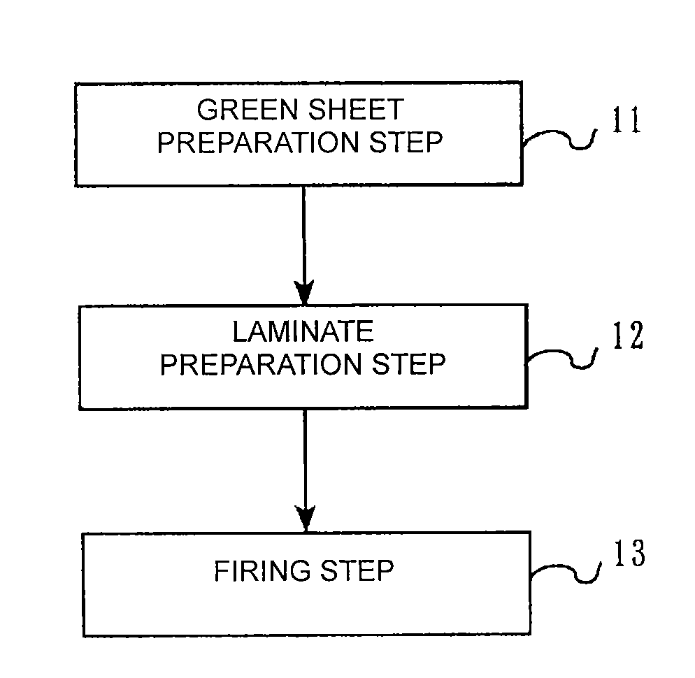
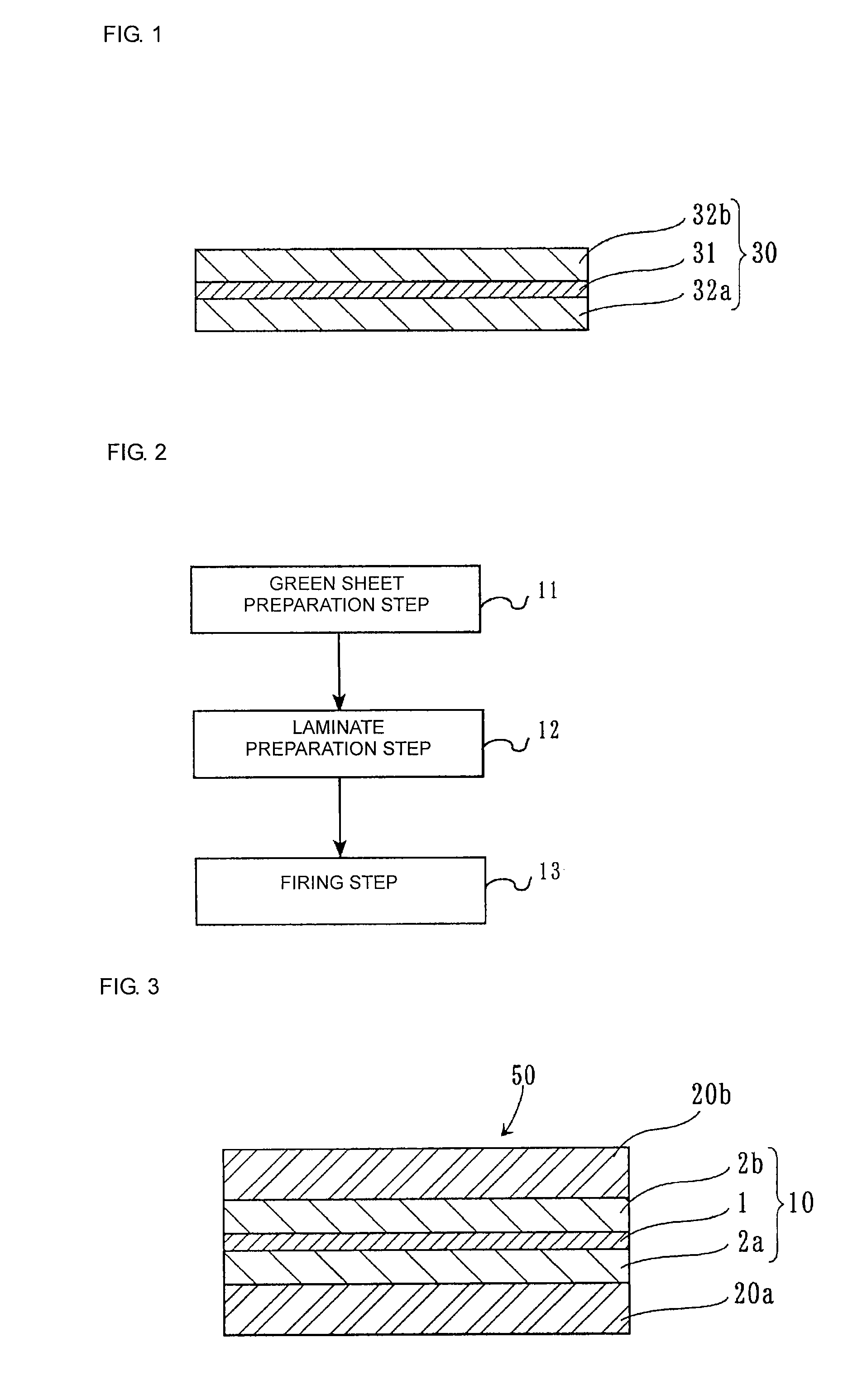
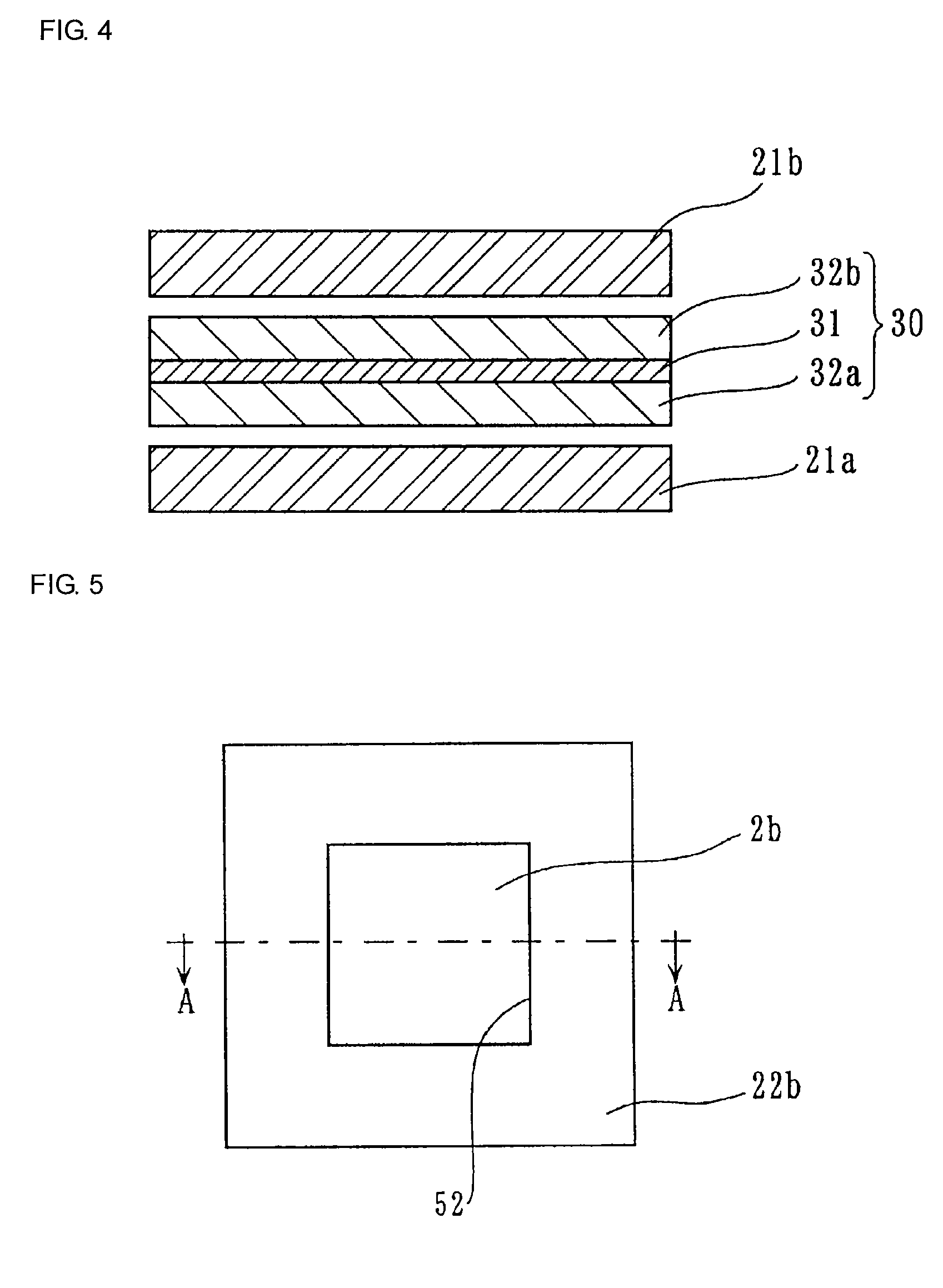
(1) Green Sheet Preparation Step

[0082]A dielectric ceramic powder mainly composed of (Ba, Ca) TiO3 and having an average particle diameter of 0.2 μm and an organic binder mainly composed of polyvinyl butyral resin were mixed and dispersed in an organic solvent containing toluene and ethanol at a volume ratio of 1:1 to prepare a dielectric ceramic slurry. The volume ratio of the dielectric ceramic powder to the organic binder to the organic solvent was 10:10:80. The volume of the dielectric ceramic powder was determined by measuring the weight of the dielectric ceramic powder and dividing the weight by its theoretical density. The dielectric ceramic slurry was formed into a sheet by a doctor blade technique to obtain a dielectric green sheet having a thickness of 2 μm.

[0083]A Ni powder, serving as the metal powder, having an average particle diameter of 0.5 μm and an organic binder mainly composed of polyvinyl butyral resin were mixed and dispersed in an organic solvent containing to...


PUM

PropertyMeasurementUnit
temperatureaaaaaaaaaa
particle diameteraaaaaaaaaa

Abstract

A dielectric green sheet containing a dielectric ceramic powder, conductor green sheets containing a metal powder, and firing-assisting green sheets containing an inorganic oxide material powder are prepared, and the firing-assisting green sheet, the conductor green sheet, the dielectric green sheet, another conductor green sheet, and another firing-assisting green sheets are stacked in that order to prepare a laminate. The laminate is then fired. During firing, the bonding strength of the interfaces between the conductor green sheets and the firing-assisting green sheets is decreased and the oxygen partial pressure of the firing atmosphere is changed at least once so that the capacitor portion is separated from the firing-assisting green sheets. In this manner, a method for manufacturing thin film capacitor by which a high-reliability thin film capacitor can be produced at high efficiency and low cost without adversely affecting the characteristics of the thin film capacitor.

Description

CROSS REFERENCE TO RELATED APPLICATIONS[0001]The present application is a continuation of International Application No. PCT / JP2006 / 308563, filed Apr. 24, 2006, which claims priority to Japanese Patent Application No. JP2005-137187, filed May 10, 2005, and Japanese Patent Application No. JP2005-206942, filed Jul. 15, 2005, the entire contents of each of these applications being incorporated herein by reference in their entirety.FIELD OF THE INVENTION[0002]The present invention relates to a method for manufacturing a thin film capacitor for use in an electronic circuit.BACKGROUND OF THE INVENTION[0003]According to the existing art, a thin film capacitor for use in an electronic circuit is made by sequentially depositing a lower conductor, a dielectric thin film, and an upper conductor on a silicon (Si) substrate. When a thin film capacitor is made by such a method, the thickness of the capacitor cannot be reduced to the thickness or less of the Si substrate, which does not contribute ...

Claims


Application Information

Patent Timeline
Patent Type & Authority Patents(United States)
IPC IPC(8): C03B29/00C04B33/32B29C65/00H01G4/33
CPCH01G4/1209H01G4/33H01G4/12H01G13/00
Inventor MINAMIKAWA, TADAHIROMAEDA, ATSUYOSHI
Owner MURATA MFG CO LTD
Why Eureka
Try Eureka