Lapping of gold pads in a liquid medium for work hardening the surface of the pads

a technology of gold contacts and liquid medium, which is applied in the direction of semiconductor devices, semiconductor/solid-state device details, electrical apparatus, etc., can solve the problems of slurries generating a large number of particles, affecting the performance of final devices, and so as to reduce the short circuit between probe wires and avoid the effect of slurries affecting the final device performance and reducing the number of particles

Inactive Publication Date: 2006-09-21
WESTERN DIGITAL TECH INC
View PDF39 Cites 2 Cited by
  • Summary
  • Abstract
  • Description
  • Claims
  • Application Information

AI Technical Summary

Benefits of technology

[0012] It is a further advantage of the present invention that gold pad surfaces are not as easily damaged by contact with probe wires.
[0013] It is a still further advantage of the present invention that electrical shorts between probe wires are minimized.
[0014] It is another advantage of the present invention that alumina slurry is not used and thus embedded alumina particles in the gold contact pads are eliminated.
[0015] It is yet another advantage of the present invention that further processing steps to remove embedded alumina particles are not required.
[0016] It is a further advantage of the present invention that processing steps are simplified.
[0017] It is an additional advantage of the present invention that better bonding with solder-ball attachments can be achieved, thus producing better production yields.

Problems solved by technology

In the formation of gold pads, to which electrical leads will be connected, such surface irregularities may affect the performance of the final device and / or create problems during subsequent processing steps.
A problem with use of such slurries, however, is that the slurries generate a large number of particles from the surface being polished which must be removed and disposed of following wafer treatment.
These particles can interfere with the solder-ball bonding of the electrical leads, and thus the overall performance can be seriously degraded.
A second cleaning process may be required to rid the gold pad surfaces of these residual particles, which of course increases processing time, and reduces efficiency.
This of course disturbs the planarity of the pads and can cause irregularities in the surface finish which can degrade the contacts made with connections in the finished product.
Gouging can lead to shorting between probe wires.
It is of course undesirable for the testing process to degrade performance of the completed component.

Method used


Image

  • Lapping of gold pads in a liquid medium for work hardening the surface of the pads
  • Lapping of gold pads in a liquid medium for work hardening the surface of the pads
  • Lapping of gold pads in a liquid medium for work hardening the surface of the pads

Examples


Embodiment Construction

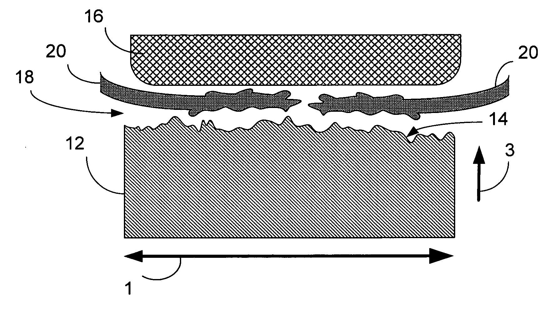
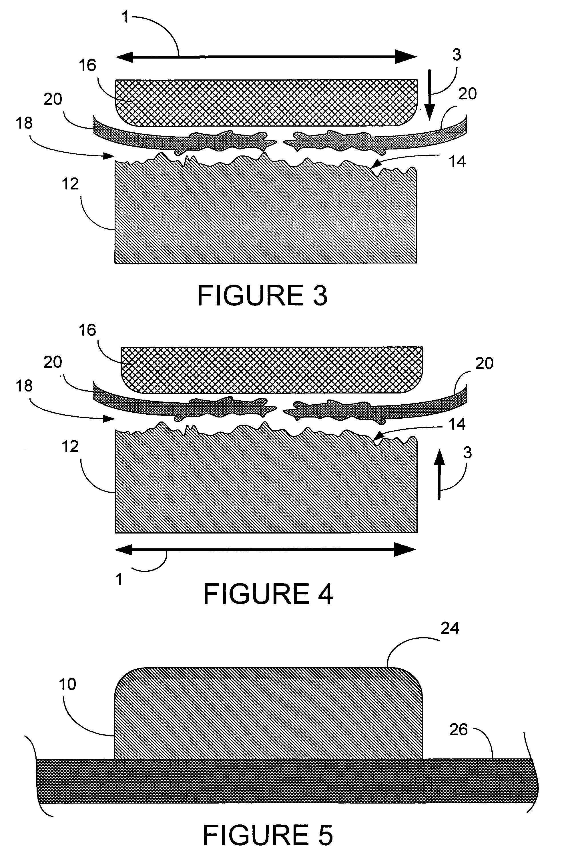
[0025] The present invention is a method for work hardening gold contact pads while applying water to the working surface, and work hardened gold pads produce by this method, which shall be represented by the element number 10.

[0026] Work-hardening is a well known technique that applies to most crystalline materials. Hardening results whenever a mechanical stress permanently dislocates atoms from their equilibrium positions.

[0027] Contact pads are used in electrical components, to make circuit connections between various leads or components. In order to make good electrical contact, the pads preferably have a smooth and planar surface. In order to prepare the pads, a lapping process is often used to smooth and planarize the upper surfaces of the contact pads. During the lapping process, mechanical stress is provided by the sheering force produced by the movement of the lapping pads relative to the contact pads. The maximum sheering force that can be generated is limited by the lub...


PUM


Abstract

A method for work hardening gold contact pads is disclosed. The method includes providing gold contact pads, providing lapping pads, and placing the lapping pads in contact with the gold contact pads to create a contact interface. A liquid medium is then applied to the contact interface while moving the lapping pads relative to the gold contact pads. The liquid medium is preferably a particulate-free pH neutral liquid, which makes water a good choice. Also disclosed is a gold pad having a work hardened surface.

Description

BACKGROUND OF THE INVENTION [0001] 1. Field of the Invention [0002] The present invention relates generally to fabrication of electronic components and particularly to lapping of gold contacts on wafers. [0003] 2. Description of the Prior Art [0004] In the fabrication of integrated circuits, a semiconductor wafer typically requires numerous processing steps, including deposition, patterning, and etching. It is often desirable to achieve a pre-determined level of surface planarity and to minimize surface irregularities such as scratches and pits. In the formation of gold pads, to which electrical leads will be connected, such surface irregularities may affect the performance of the final device and / or create problems during subsequent processing steps. [0005] Consequently, a typical process includes treatment of surface defects on the wafer surface by using a polishing pad in conjunction with slurry containing loose abrasive particles dispersed in a liquid. A problem with use of such...

Claims


Application Information

Patent Timeline
Patent Type & Authority Applications(United States)
IPC IPC(8): H01L23/02
CPCH01L24/11H01L2224/13099H01L2924/01079H01L2924/01082H01L2924/14H01L2924/01005H01L2924/01006H01L2924/01033H01L2924/014
Inventor DUNHAM, RONALDGOUBAU, WOLFGANGPATEL, BHARGAVWONG, MARVINYANG, JOHN JAEKOYUN
Owner WESTERN DIGITAL TECH INC
Why Eureka
Try Eureka